Skip to content

2026-10-08 MRVL 与 AI 互连行业研究:产品竞争、战略投资及每股现金回报 ​

  • 数据时间:MRVL 为 2026 年 10 月 7 日美股常规收盘 284.68 美元(北京时间 10 月 8 日 04:00);资产负债表截至 2026 年 8 月 1 日。[S19][S3]
  • 研究对象:Marvell Technology(MRVL),并比较 AI 计算、网络、光连接及存储链条。
  • 报告类型:首次覆盖后的专题扩展;投资期限同时检验短期事件、3–12 个月经营和 1–3 年结构性回报。
  • 资料来源:公司及竞品披露、合同原文、公开预测、具名行业研究与硬件报道。来源及访问状态见文末。

结论与建议 ​

Marvell 的数据中心业务已经形成规模,互连和定制芯片扩张有真实的产品基础;以 284.68 美元计,新增资金当前首选动作为 pass/暂不参与。 FY2027 Q2 数据中心收入 21.715 亿美元,占总收入 79.3%;公司把 FY2028 收入目标提高到 200 亿美元,FY2029 定制芯片目标提高到超过 120 亿美元。然而,公开预测中的 FY2028 收入已达 196.2 亿美元、调整 EPS 为 7.25 美元,现价约为该 EPS 的 39.27 倍。按本文 FY2029 情景估值,基准价值 318.75 美元,较收盘价高 12.0%;不利情景为 156.54 美元,低 45.0%。这组赔率尚未补偿产品量产、现金转换和股数扩张的共同不确定性。[S1][S2][S19][S20]

判断当前结论
最高优先级观点从连接芯片到 XPU 周边的内容增长具有经营价值;股票的每股现金回报需要比收入目标更强的证据。
市场隐含判断公开汇总 FY2028 收入 196.2 亿美元,距公司 200 亿美元目标约 1.9%;按分析假设固定 30 倍 FY2029 EPS、40% 营业利润率和 9.8 亿股,现价反推约 277.3 亿美元收入。这是模型反推,并非所有投资者的共同预测。[S1][S19][S20]
不同判断定制芯片、DSP、交换与内存连接可共同受益,客户权证、产品替代和研发产能投入也会分享增长收益。关键差异在新增收入能否形成扣除稀释与客户激励后的每股自由现金流。
传导机制客户资本开支经过设计资格、采购、制造、交付和付款才转为收入与现金;产品组合决定毛利率,营运资本、预付款和 SBC 决定股东所得。
观点状态与证据变化维持经营积极、股票 pass;公开 FY2028 收入预测由 183.4 亿升至 196.2 亿美元,增强增长支持,却缩小相对市场的预期差。新核合同澄清融资与权证经济权利;竞品量产、铜连接实例和 CPO 成本模型增加反证。长期兑现置信度仍为中低。多数合同及财务事实原本已发生。[S6][S20][T1][T5][S38][S39]
当前首选动作pass/新增资金不参与。MRVL 留在高优先级复核名单;现价缺少足够风险收益余量。
置信度历史财报及可取得合同条款较高;多年度产品份额和每股现金预测中低;当前动作中等。
主要依据Q2 与半年现金流、FY2028 预测与收盘价、Google 权证、按产品层级的竞品披露及非官方反方研究。[S2][S3][S19][S20][T5][S38][S39]
最大反证如果 FY2031 接近公司 800 亿美元收入中点,达到约 45% 营业利润率,股数控制在 10 亿股且终值倍数仍为 30 倍,本文长期牛市参考现值约 608 美元;谨慎判断可能错过大幅上涨。[S1]
失效条件任一正式下调 FY2028 收入 200 亿美元目标、FY2029 Custom 超过 120 亿美元目标,或主要设计项目退出,均要求重建经营假设;现金转化持续弱于增长、净股数超出情景则分别重估现金与估值分母。
下一验证FY2027 Q3 的 31.5 亿美元±5% 收入指引及 CFO−capex、SBC、预付与股数;T100、Structera、Ara 与 PhotonicFabric 的客户资格、生产收入和净现金贡献。Q3 披露确切日期尚未核实。[S2][S10][S23]
条件式框架接近 230–250 美元时重算收入、正常化 FCF 与股数,而非因股价本身升级;现价若要转为试探参与,需要更高且有证据支撑的基准回报空间。

公司与行业:增长从何而来 ​

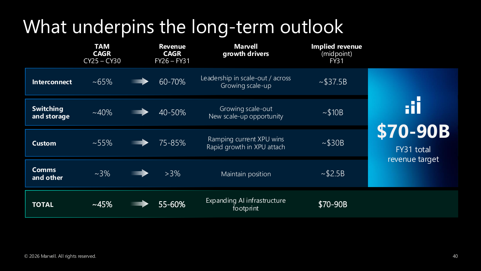
Marvell FY2026 收入约 82 亿美元;公司给出 FY2027 约 120 亿、FY2028 200 亿美元,FY2031 700–900 亿美元的管理层规划。FY2031 的 800 亿美元中点由互连 375 亿、交换与存储 100 亿、定制芯片 300 亿、通信及其他 25 亿美元组成。从 FY2028 的 200 亿至中点仍需约 58.7% 的三年复合增速,单靠产品规格提升无法完成。[S1]

Marvell 投资日第 40 页:FY2031 收入中点及业务目标

投资日用“连接约 70%、计算约 30%”概括技术敞口;财报披露的仍是数据中心与其他终端市场,不能把这两个比例当作已报告的收入分部。数据中心 Q2 收入 21.715 亿美元;公司称前四大超大云厂商有多代定制合作,但没有逐客户、逐芯片收入、不可撤销采购额和产品级 ASP。FY2026 前十大客户(含分销商与直接客户)贡献 82% 收入,因此客户项目延后会明显影响路径。[S1][S2][S3][S7]

客户投资提供需求背景。Microsoft FY2026 Q4 季度资本开支 410 亿美元;Alphabet 2026 Q2 资本开支 449.24 亿美元;Amazon AWS 当季收入 422 亿美元;Meta 的年度资本开支指引为 1,300–1,450 亿美元。这些金额有不同资本化和租赁口径,支出还覆盖 GPU、建筑、电力与网络,不能按固定比例归给 Marvell。Alphabet 当季自由现金流为负,也提示大客户最终会考核投入回报。[S14][S15][S16][S17]

八层产品竞争:规格、阶段与价值捕获 ​

领域Marvell 产品与阶段主要竞争路线决定客户采购的变量
Custom XPU、周边 ASIC服务客户 XPU,以及定制 NIC、内存、安全、存储等 XPU attach;公司预计 FY2031 Custom 中两部分大致平衡。[S1][S7]Broadcom 已报告 FY2026 Q3 AI 半导体收入 167 亿美元;MediaTek 宣传 7–2nm 70 多次 tape-out;Alchip 披露 2nm 开发进展。[S11][S33][S34]芯片归属、设计复用、先进封装、可量产良率和客户内部设计深度。不同客户项目收入未披露,无法据设计胜利直接计算份额。
NIC/DPUOCTEON 10、OCTEON 10 Fusion 面向数据处理和定制计算;FastLinQ 为另一代网卡产品线。[S1][S44]NVIDIA ConnectX-8 的 800Gb/s 为双 400G 总吞吐,ConnectX-9 的每 GPU 1.6Tb/s 属平台口径;AMD Vulcano 标注每 NIC 800Gb/s。[S26][S27]主机与网络协议、DOCA 等软件生态、卸载功能、每 GPU 配置和客户绑定。不得以平台总吞吐对照单卡端口。
以太网交换Teralynx T100 标注 102.4Tb/s、3nm,2026 年 6 月公告称当季送样;FY2028 scale-out 交换收入目标超过 10 亿美元。[S1][S10]Broadcom Tomahawk 6 同为 102.4Tb/s,公告称已批量生产;其 Jericho、Tomahawk Ultra 和 Davisson CPO 覆盖不同拓扑;NVIDIA Spectrum-X 提供平台组合。[S12][S21][S26]产品送样转生产的时间、拥塞与软件、端口功耗、完整系统价和开放互操作。T100 宣称的最多 25% 节能缺少同条件第三方测试。
PCIe/CXL 交换、内存池Structera S 60260 为 PCIe 6.0 的 260 lane,其中 256 为数据、4 为管理;3 月有工程样片并预计 Q3 客户采样。Structera A/X/S 面向近内存加速、扩展与池化。[S23][S28]Astera Scorpio X-Series 320 lane memory-semantic fabric 公告称已出货,P-Series 是 32–320 lane PCIe 家族;Microchip Switchtec Gen6 有最高 160 lane HLC。[S24][S25]协议语义、拓扑跳数、内存一致性、软件和交付阶段。Astera 的 X 系列出货不能证明全部 P 系列量产;Marvell 3 月的采样预期仍需事后确认。
有源铜缆/光模块 DSPAra、Ara T、Ara X、Petra 1.6T 被投资日列为当前出货,Ara M 接近推出;Ara T 的 TRO 发端处理面向 5–500 米。[S1][S43]Broadcom 展示 400G/lane Taurus;Credo 的 1.6T ZeroFlap 将 DSP、Kfir200 硅光芯片与 PILOT 诊断结合。[S21][S22]相同距离与端口下的误码、模块功耗、可靠性、互操作、售价及诊断成本。Marvell“模块省电超过 35%”是厂商比较口径。[S43]
相干 DSP/DCI 模块商用 DSP 与 COLORZ 模块是两种不同销售层级;2nm 3.2T PAM、coherent-lite 为演示,1.6T ZR 与 800ZR MACsec 亦在展示。[S1][S9]Cisco/Acacia CIM8、Jannu,Ciena WaveLogic 6e/6n。Acacia 1.2T faceplate 与 Ciena 1.6T 单载波对应不同距离和模块配置。[S31][S32]每公里距离、模块密度、完整功耗、标准与运维。ISSCC 报道的 Marvell coherent-lite 800G、40km、3.72pJ/bit 未计硅光功耗,属于会议器件口径。[S40]
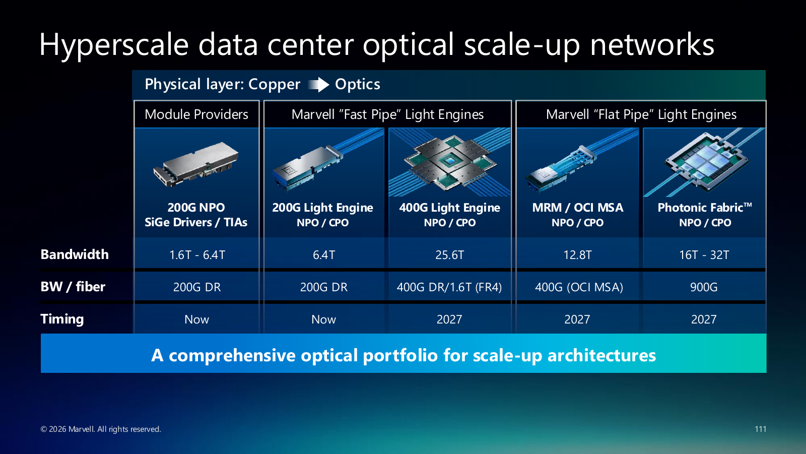
NPO/CPO、光引擎FastPipe 200G light engine 6.4T 标注当前,400G/25.6T、OCI 12.8T 和 PhotonicFabric 16–32T 为 2027 路线;scale-up 光学现有收入接近零。[S1][S7]Broadcom Davisson、NVIDIA 集成 CPO、Ayar TeraPHY+SuperNova 外置激光及传统可插拔方案同时竞争。[S21][S35][S39]光纤装配、封装良率、激光器供给、故障影响范围、现场维护与整座集群成本。新光收入需要扣除被替代的可插拔 DSP 内容。
SSD 控制器Bravera SC5 的公开规格为 PCIe 5.0/NVMe 1.4b、8/16 NAND 通道,属于 2021 年历史产品资料;公司还列有定制 SSD 控制器。[S1][S29]Silicon Motion MonTitan SM8366/SM8308 为 Gen5、production-ready,提供控制器、固件与参考方案。[S30]终端 SSD 厂商自研/外购、固件可靠性、NAND 适配与量产认证。Marvell 销售控制器或设计服务,不能把 SSD 整盘与 NAND 销售额归入其收入。

PCIe 两家产品尤其容易误比:Marvell 的 260 lane 包括管理通道;Astera 320 lane X-Series 使用 memory-semantic fabric,P-Series 才是 PCIe 系列。只有相同协议、网络规模、负载、软件和商业阶段下,lane 数量才开始有性能意义。ServeTheHome 对 Scorpio 的解读说明更大连接预算可减少级联跳数,但其拓扑图来自 Astera 材料,缺独立的系统价格及每瓦吞吐。[S23][S24][S37]

Marvell 投资日第 111 页:scale-up 光引擎与产品窗口

非官方研究带来的反方检验 ​

SemiAnalysis 的 CPO 模型把器件和系统分开:按其假定配置,800G 的 CPO 光引擎及外置激光器约 4–5W,对照传统 DSP 光模块 16–17W;三层 GB300 NVL72 网络中,网络功耗下降约 23%,整座集群功耗仅下降约 2%,成本约下降 3%。改成两层网络时整群功耗模型降幅约 4%。参数含网络拓扑、组件价格和利润假设,属于作者测算。其引用的 Meta 小规模端口小时实验比宣传规格更接近使用数据,但仍不足以定出大规模现场故障率。[S39]

ServeTheHome 对 AMD Helios 网络托盘的分析则提供铜连接仍被选用的具体案例:其解读是该方案使用 Broadcom Tomahawk 6 和铜互连,原生 UALink 交换产品的可用时点与成本功耗取舍影响设计。这份资料只覆盖所读网络托盘页面,说明某代平台选型,未显示 Marvell 失去项目。[S38] 该媒体 2024 年访问的 Teralynx 10 交换机提供端口及机箱实物观察,但 Marvell 赞助了行程;约 500W 芯片与 1.8kW 光模块是说明性估值,并无 T100 对 Tomahawk 6 的实验室功耗对比。[S36]

LightCounting 创始人 Vladimir Kozlov 在 2026 年 1 月公开摘要中把客户批准和多供应商生态列为 CPO 扩大的关口。其文章全文需另行登录;摘要对单个云厂规划的描述也只是当时行业判断。[S41] Asia Tech Research 10 月 1 日匿名问答称 Marvell 部分 1.6T DSP 面临良率与功耗压力,并对 Broadcom 出货作高量预测;没有型号、测试条件或订单。OCP 材料显示 Ara MV-CD833 是 TSMC 3nm,足以提醒匿名“多数采用 Samsung”说法不能覆盖所有 Ara 型号,但不足以证明其他型号无供应问题。该问答只形成待核验问题,没有进入本文收入和份额估值。[S42][S45]

行业机构、具名作者、厂商演示和独立测量各提供不同类型的信息。此时最有决策价值的是产品从演示、工程样片、客户采样、出货到批量生产的进程,以及同一距离/拓扑下可重复的每瓦成本,而非把各方最大的速率数字排成榜单。

大型企业外部投资:金额、价格与可售时间 ​

战略资本正在进入定制芯片、激光/光模块、互连材料和设计软件。下表按发行人取得的现金、证券权利和合同可转让条件列示;价格为投资或行权条款,不代表目前市价。仅写已经取得证据的交割状态。普通股投资、可转优先股与客户权证的经济权利差别很大。[T1][T5][T7][T9][T11][T13][T14][T15]

投资方 → 发行人金额、交割证券与约定价格锁定/可售节点与已知状态
NVIDIA → Marvell20 亿美元已于 2026-03-31 交割200 万股 A 类可转优先股,每股 stated value 1,000 美元;初始每股约可换 10.889 股普通股,初始普通股换股价约 91.8355 美元,共约 2,177.8 万股。[T1][T2]2026-08-01 财报时仍为优先股。自愿转换需满足适用 HSR 等条件;完整购买协议未取得,合同锁定和转售登记截止日未知。[T2][T6]
Google → Marvell无同类现金股权投资额;商业协议 2026-07-29 签署,权证 08-18 发行最多 5,897.0907 万股,行权价 206.58 美元,通常 2033-08-18 17:00 加州时间到期;其中 136.0867 万股按时间、5,761.004 万股按合格采购归属。[T4][T5]时间归属部分的转让限制见下方时间轴;实际归属、行权、股份发行、登记生效与出售未查到完成记录。
NVIDIA → Coherent(COHR)20 亿美元已于 2026-03-02 交割778.8161 万股普通股,256.80 美元/股。[T7]公司后续文件披露交割后六个月合同锁定,机械届满日 2026-09-02;书面同意例外及登记条件仍影响可售性,实际出售未知。[T8]
NVIDIA → Lumentum(LITE)20 亿美元已于 2026-03-02 交割287.6415 万股可转优先股,695.31 美元/优先股,初始约 1:1 换普通股。[T9][T10]自愿转换受 HSR 条件约束;现有证据未给可核实的合同解禁和转售登记日期。
NVIDIA → Intel(INTC)50 亿美元,2025-09 签约,2025-12-26 已交割2.14776632 亿股普通股,23.28 美元/股。[T11][T12]未取得交易专属锁定与转售登记条款;不能借其他交易的六个月安排推定 Intel 可售日。
NVIDIA → Synopsys(SNPS)20 亿美元的 2025-12-01 认购协议;本次材料仅确认签署482.1717 万股普通股,414.79 美元/股。[T13]交割及现金到账、锁定和登记日期尚未核实。
NVIDIA → Corning(GLW)5 亿美元购买两类权证,2026-05-06 披露发行传统权证 1,500 万股、行权价 180 美元;预付型 300 万股、行权价 0.0001 美元。[T14]一般可自发行时行权、最长约三年且可提前终止。传统权证全额行权的另 27 亿美元仅是潜在后续款;转售约束未知。
Amazon → Astera Labs(ALAB)客户采购权证,非本次现金投资;2026-02-05 发行最多 326.2299 万股,行权价 142.82 美元,正常到期 2033-02-05;随指定产品合格采购付款逐步归属,上限 65 亿美元。[T15]详细分档及股份可售日未完整取得;65 亿是归属计量上限。现有 8-K 还提到 2022 年权证与 2023 年修订。

这一组交易不能相加为 Marvell 订单或半导体行业的“净新增需求”。NVIDIA 的现金同时改善供应商融资能力并取得权益;Google、Amazon 的客户权证则把未来业务拓展与发行人现有股东权益联系起来。对 Marvell 股东,应分别核对客户净收入、生产利润、现金回收与最终股份数。

Google 权证:归属、限制转让、行权与出售四个时钟 ​

Google 的 136.0867 万股时间归属部分按发行日后 3、6、9、12 个月分四档。其余 5,761.004 万股分 240 档:前 239 档各 240,042 股、最后一档 240,002 股;每档需要再增加 5 亿美元合格 Custom 产品收入,计量期为 2026-08-01 至 2033-01-29。因此全部业绩部分归属对应累计 1,200 亿美元计量门槛。合格收入依协议以 GAAP 产品收入为基础,扣除返利退款并按合同排除权证造成的 contra-revenue 项;购买规模由 Google 决定。[T5]

节点适用份额/条件投资含义
2026-11-1834.0216 万股首档时间归属,按发行日机械推算是潜在归属节点;截至报告日尚未发生,不构成对外销售许可。
2027-02-18、05-18、08-18各 34.0217 万股后续三档,按合同月份机械推算需要逐次核对实际生效和后续行权。
2027-11-10 或 Kestrel Product Launch 较早者仅时间归属部分的合同转让限制。Kestrel 定义为最终量产版本通过产品资格认证合同把 2027-11-10 括注为发行后 15 个月,与 2026-08-18 发行日的月份算术不一致;保留明确写出的日期,待正式澄清。实际 Kestrel 资格认证日期未知。
单日卖出限制一般不超过此前 10 个交易日平均成交量的 10%,包销公开发行或大宗交易例外;适用于全部权证股份只有实际持有可售股份时才涉及卖出容量,不能据此预报每日抛压。
登记、行权与到期持有人书面请求后 60 天内提交转售 shelf;生效需合理商业努力,没有固定生效日。已归属股份可按 206.58 美元行权,通常 2033-08-18 到期,可有合同延期机制提交、生效、行权、发股及出售须单独证明。最高全部现金行权价款约 121.82 亿美元属于假设资金流,现金less行权亦可能改变资金与股数。

Google 权证最高名义股数占 10 月 7 日普通股数约 6.72%。若假设全部归属、当前价不变且可行权,按 284.68 美元作库存股法示意,净增约 1,617.8 万股;这个数字随股价和实际归属变化。合同权证的收益、会计处理和持股稀释均需追踪,尤其不能同时把 1,200 亿美元写成已承诺采购,再忽略客户获得的权益。[S19][T5]

财务、资本投入与每股经济性 ​

FY2027 Q2 收入 27.390 亿美元、GAAP 营业利润率 16.8%、净利润 3.080 亿美元;调整营业利润率 36.6%、调整净利润 8.659 亿美元和 EPS 0.94。季度股权薪酬(SBC)3.262 亿美元,无形资产摊销 2.149 亿美元。调整利润展示经营规模,SBC 的股东代价还需在后续股数和现金决策中体现。[S2]

指标FY2027 Q2FY2027 上半年FY2031 公司规划
收入27.390 亿美元51.565 亿美元700–900 亿美元
CFO6.055 亿美元12.443 亿美元未披露绝对金额
Capex1.267 亿美元2.824 亿美元未披露绝对金额
CFO−capex4.788 亿美元9.619 亿美元FCF 率 超过 36%
上述 FCF/收入17.48%18.65%目标 超过 36%
SBC3.262 亿美元5.338 亿美元未给出逐年预算
调整营业利润率36.6%—44–46%

上半年 CFO−capex 为 9.619 亿美元,同期 SBC 5.338 亿。两者的 4.281 亿美元差额仅是股权薪酬经济性诊断:会计 CFO 本身已加回非现金 SBC,未来每股估值若已反映净稀释,就不能再机械扣一遍全部 SBC。经营现金流同时受 6.603 亿美元营运资金流出、4.12 亿美元应收账款无追索保理影响。产能预付从期初 2.788 亿增至 4.870 亿美元,代工与封测采购承诺 85.189 亿美元。管理层的长期 36% 以上 FCF 率仍需要利润扩张、回款和投资效率共同兑现。[S1][S2][S3]

Celestial AI 收购购买对价公允价值约 35 亿美元,其中 upfront 约 13 亿现金及 2,450 万股;至 FY2029 还可能支付最多 2,240 万股和 2.33 亿美元现金,期末或有对价负债 7.495 亿美元。XConn 对价约 4.69 亿美元。产品路线因此增加,但采购、预付、并购、研发和股权激励需要共同进入增量资本回报检验。已记录的或有负债与未来或有股份不能在企业价值中重复扣减。[S3]

资本结构必须按时点桥接。 2026 年 8 月 21 日普通股约 8.769 亿股,10 月 7 日第三方股数统计为 8.7693 亿股;按 284.68 美元,普通股权益约 2,496.44 亿美元。用 8 月 1 日账面现金 39.328 亿、债务 49.629 亿和经营租赁负债 3.232 亿合并,普通股企业价值示意约 2,509.98 亿美元,这是混合时点参考。[S3][S19]

NVIDIA 的 20 亿美元已计入这笔现金。优先股初始等效约 2,177.8 万普通股,若静态加到上述普通股,得到约 8.98708 亿股的普通股+优先股换股参考;FY2027 Q2 报告的加权摊薄 9.212 亿股已经包括约 2,180 万优先股换股影响和奖励/其他权证。因此不能在 9.212 亿上再次叠加 NVIDIA 的 2,177.8 万股,也不能同时把这 20 亿作为新现金再加一次。Google 权证晚于 Q2 报表日发行;未来股数还受奖励、Celestial 或有股份和回购左右。[S3][T1][T2]

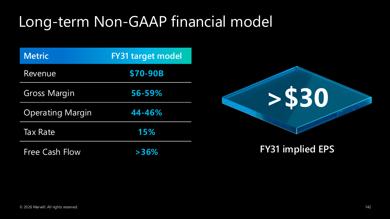
Marvell 投资日第 142 页:FY2031 调整利润和 FCF 目标

估值与机会成本 ​

本文用 FY2029 调整盈利乘情景市盈率,描述未来 12–24 个月可能给出的前瞻价格;营业利润、净利息、税率、股数和倍数均为分析假设。基准收入 310 亿美元拆为互连 135 亿、Custom 125 亿、交换与存储 30 亿、其他 20 亿;40% 营业利润率、1.5 亿美元净利息、15% 税率和 9.8 亿股得到 EPS 10.625 美元,乘 30 倍约 318.75 美元。基准收入仍较 FY2028 公司目标高 55%,需要继续放量。[S1]

FY2029 情景收入营业利润率股数EPS情景 P/E前瞻价格较 284.68 美元
不利240 亿美元35%10.0 亿6.81 美元23 倍156.54 美元−45.0%
基准310 亿美元40%9.8 亿10.63 美元30 倍318.75 美元+12.0%
有利360 亿美元43%9.8 亿13.34 美元34 倍453.55 美元+59.3%

利润率和股数改变很快侵蚀基准空间。收入仍为 310 亿、30 倍估值时,营业利润率降至 35%,前瞻价格约 278.42 美元;营业利润率保持 40% 而股数升至 10.5 亿股,价格约 297.50 美元。按同样的 40% 利润率、9.8 亿股与 30 倍反推,现价对应 FY2029 收入约 277.3 亿美元。这是能解释现价的一组模型参数,未观察到统一市场信念。[S19]

现金流交叉检查更加严格:假设 FY2029 收入 310 亿美元、股数 9.8 亿、给予正常化 FCF 30 倍,20%/25%/30% FCF 率对应约 189.80/237.24/284.69 美元。现价需要约 30.0% 的正常化 FCF 率;上半年实际为 18.65%,公司 FY2031 目标为超过 36%。这两端分别是当前历史和多年规划,维护与增长 capex、客户激励、营运资金及净股数仍未完整拆出。[S1][S2][S3]

FY2031 约束情景收入/调整营业利润率股数、终值 P/E、股权要求回报2031-01-31 每股终值折回 2026-10-08 参考值
不利350 亿美元/35%10.5 亿股、20 倍、15%190.50 美元104.23 美元
基准600 亿美元/42%10.2 亿股、26 倍、12%543.83 美元333.50 美元
有利800 亿美元/45%10.0 亿股、30 倍、10%918.00 美元608.47 美元

长期情景用约 4.31 年把终值折至报告日,省略中途分红;它是 EPS 倍数终值检验,并非完整 DCF,也不与上表 12–24 个月前瞻价格混为一个目标价。公司 FY2031 中点 800 亿与调整 EPS 超过 30 美元为管理层目标,本分析长期基准 600 亿美元低于该目标。若坚持 26 倍、42% 营业利润率、10.2 亿股和 12% 折现,现价反推 FY2031 收入约 512.5 亿美元。[S1]

目前没有同期、同口径的同业股价和分部利润数据,本文不制作伪精确的“同行平均倍数”。Broadcom 的 FY2026 Q3 AI 半导体收入和交换芯片量产提供强竞争锚,但其合并 FCF 包含软件。Credo 的 FY2027 Q1 收入 4.79 亿美元、次季指引 5.25–5.35 亿美元,提示 AEC/光模块竞争已有增长;仍须按芯片、模块和系统收入层级比较。[S11][S12][S13]

三个期限的机会判断 ​

期限有效问题MRVL 当前动作与重新检验条件
数周至三个月:财报事件Q3 收入能否进入 31.5 亿美元±5% 指引、调整 EPS 1.10±0.05,同时 CFO−capex 与净股数改善?披露日尚未核实。[S2]pass。只凭数字达到指引仍需核对现金及 FY2028 路径;事件失利对当前高倍数有重估风险。
三至十二个月:经营预期差Ara、T100、Structera 的客户资格和生产收入能否超越公开 FY2028 收入预测 196.2 亿美元,同时保持利润与现金质量?[S10][S20][S23]观察候选。公开预测已接近公司 200 亿美元目标;只有可归属的收入/现金超预期或显著改善的价格赔率才考虑试探。
一至三年:结构性行业机会Custom attach、光连接与交换扩张是否带来可持续每股现金增长,且客户权证、并购及产品替代成本可控?[S1][S3][T5][S39]观察候选。规模化生产、净稀释和资本回报得到较强验证且估值保留余量时,才讨论更高确信度。

同链条还有 Broadcom 的既有交换与 ASIC、Astera 的服务器互连、Credo 的短距连接及 Coherent/Lumentum 的光学能力。它们是后续相对价值复核的候选,不因产品增长就推断股票便宜;本期缺少同日可比价格、盈利和现金估值,当前资本选择为保留新增资金。未观察到足以建立各候选相互独立收益分布的证据,产业共同受云厂资本开支影响。[S11][S13][S22][S24][T7][T9]

监控雷达与观点失效 ​

验证点已知锚点与下一步影响
财报与年度路径FY2027 Q3 公司指引收入 31.5 亿美元±5%、调整 EPS 1.10±0.05;下一次正式披露核对收入、订单交付与 FY2028 目标。[S2]正式下调 FY2028 200 亿目标或 FY2029 Custom 超 120 亿目标,分别重建对应收入情景。
现金与股本H1 FCF 率 18.65%、SBC 5.338 亿美元、营运资金流出 6.603 亿;逐季核对 CFO、capex、保理、预付款、加权与期末股数。[S2][S3]收入增长若持续未转化为正常化 FCF/股,降低倍数和股数假设。
商业化级别T100 客户采样至量产,Structera 客户资格,Ara/coherent-lite 实际出货,2027 光引擎路线。[S1][S10][S23]型号、客户、可核实收入、毛利与系统成本同向改善,才上调基准。
Google 与并购经济性权证实际各档归属、Kestrel 资格、contra-revenue、Celestial 或有支付和实际发股。[S3][T5]调整客户净利润与稀释桥;合同日期冲突以正式补充文件澄清。
架构替代Helios 的铜/TH6 路线,CPO 大客户采用、维修、激光供给与整群 TCO。[S38][S39][S41]若可插拔 DSP 内容减少而 Marvell 未赢得替代光引擎项目,调低互连增长和利润率。

快讯、文章与研报页内阅读 ​

文章与研报 ​

来源发布日期站内阅读状态
Stock Analysis2026-10-06MRVL上调AI连接增长目标原文与中文摘要已归档
NVIDIA2026-03-31英伟达与Marvell加深AI合作原文与中文摘要已归档
Marvell2026-09-21Marvell披露2纳米光互连演示原文与中文摘要已归档
Marvell2026-06-01Marvell公布Teralynx T100交换芯片原文与中文摘要已归档
Broadcom2026-03-12Broadcom Now Shipping World’s First 102.4 Tbps Switch in Production Volume正文未取得:Extractor returned too little article text
Broadcom2026-09-02Broadcom AI半导体收入大增原文与中文摘要已归档
Credo未提供Q1收入4.79亿美元,同比+114.7%;调整毛利率68%;Q2指引5.25-5.35亿美元。(正文未取得)正文未取得:HTTP 403
Amazon未提供AWS收入422亿美元,同比+37%,营业利润166亿美元。(正文未取得)正文未取得:Extractor returned too little article text
Meta未提供Q2收入608亿美元,+28%;capex310.8亿美元(含融资租赁本金)、FCF7.84亿美元;CY26capex指引1300-1450亿美元。(正文未取得)正文未取得:HTTP 403
Microsoft2026-07-29微软扩建AI算力并提高资本开支原文与中文摘要已归档
Broadcom2026-03-11Taurus为400G/lane optical DSP演示;TH6 102.4T公告称production volume;Davisson CPO、Tomahawk Ultra、Jericho4、Thor Ultra 800G NIC列入展示组合。(正文未取得)正文未取得:Extractor returned too little article text
Credo2026-09-16Credo将可靠性诊断扩展至1.6T光模块原文与中文摘要已归档
Astera Labs2026-05-05Astera发布320通道Scorpio交换芯片原文与中文摘要已归档
Patrick Kennedy / ServeTheHome2024-07-22Teralynx 10交换机的端口与功耗配置原文与中文摘要已归档
Vic A / ServeTheHome2026-05-05STH解释Scorpio的高通道数拓扑价值原文与中文摘要已归档
Ryan Smith / ServeTheHome2026-08-03AMD Helios采用Broadcom铜互连网络原文与中文摘要已归档
Dylan Patel / Daniel Nishball / Myron Xie 等2026-01-01CPO经济性与Celestial光互连路径原文与中文摘要已归档
SemiAnalysis2026-05ISSCC光互连与先进封装进展原文与中文摘要已归档
Vladimir Kozlov / LightCounting2026-01-27CPO大规模部署待云客户批准原文与中文摘要已归档
Asia Tech Research2026-10-011.6T光DSP供应与竞争预测原文与中文摘要已归档
Henry Chen / Marvell2026-03-16Ara T以单向DSP降低模块功耗原文与中文摘要已归档
Reddit r/ValueInvesting 公开账号,见原文2026-10-07投资日后的公开讨论正文未取得:HTTP 403
打开原文

MRVL上调AI连接增长目标

重要性5/5 高

公司直接上调FY2028营收目标,并提供FY2029定制业务与FY2031收入、利润率和现金流目标;问答对大型协议纳入程度及增长约束作了补充。

中文摘要

核心结论

Marvell在2026年10月6日投资者日把FY2028营收目标提高至约200亿美元,并提出FY2031营收700亿至900亿美元、非GAAP(非通用会计准则)每股收益超过30美元的长期目标。管理层将增长归因于数据中心互连、交换/存储及定制芯片;目标能否兑现取决于客户项目量产、资本开支和供应链执行。

重要性评级

5/5(高):这是MRVL年度投资者日,公司上调近期开支周期内的营收目标,并给出FY2029定制业务和FY2031营收、利润率与现金流框架;问答还说明大额协议机会如何进入预测。

关键事实

  • 管理层估算,CY2030 Marvell可服务市场(TAM)约4000亿美元,2025至2030年复合增速约45%;其采用的数据中心资本开支假设约3万亿美元,复合增速约35%,并预计周期后段放缓至约20%。这是公司市场测算,不代表已取得收入。
  • FY2028总营收目标升至约200亿美元,其中数据中心约180亿美元;公司称较FY2026的82亿美元总营收增长显著。FY2029定制业务目标提高至超过120亿美元,管理层称从FY2028水平增长逾三倍。
  • FY2031总营收目标为700亿至900亿美元,数据中心约675亿至875亿美元;中点800亿美元按业务分为互连375亿美元、交换与存储100亿美元、定制300亿美元、通信及其他25亿美元。目标区间对应公司所述总营收复合增速约55%至60%。
  • 定制业务涵盖XPU(AI加速器)及XPU attach(围绕加速器的定制配套芯片),包括网络接口、内存扩展、存储、服务器管理和推理加速。管理层称FY2031业务将由XPU与配套芯片较均衡构成,且不依赖单一插槽;这是基于公司所称的设计项目和客户关系作出的预测。
  • 公司称机柜内扩展(scale-up)光学业务当前收入接近零,预计下一财年开始显著放量;CEO在问答中称初期规模可达数亿美元。近封装光学(NPO)与共封装光学(CPO)将并行推进。公司同时称100T以太网交换芯片已有产品发布,51.2T交换业务预计下一财年超过10亿美元;这些是不同业务和进度,不能把交换收入目标当作光学收入。
  • 管理层称Google的TPU相关定制协议勾勒出六年半累计约1200亿美元的机会,且与现有连接业务分开。CEO在问答中称FY2031定制业务模型只纳入近期大型协议机会的一部分,按其判断的较可能情形估算;1200亿美元是公司描述的机会规模,不能视为已签订单或确定收入。AI实验室相关业务被CEO称为潜在上行选项。
  • CFO给出的FY2031目标为毛利率56%至59%(受产品组合影响)、营业利润率44%至46%、税率15%、自由现金流率超过36%,以及非GAAP每股收益超过30美元。公司计划长期平均返还超过50%的自由现金流,同时继续投入增长并维持灵活资产负债表。CFO回顾FY2021至FY2026约80亿美元研发投入、110亿美元并购投入及约40亿美元股息和回购;演讲没有给出FY2031股数、稀释假设或未来回购金额。

作者观点与证据

这是Stock Analysis发布的投资者日演讲及问答转录,主要证据是Marvell管理层陈述。管理层称前十大云客户占数据中心资本开支比重将继续上升,公司已在多代产品上取得设计项目,并已为增长安排供应链产能;转录未附客户合同、订单明细或独立验证材料。问答中,CEO称公司预测假设资本开支逐步放缓,FY2031定制模型按“较可能”情形估算,并非把大型协议的最大潜力全部计入。关于土地、电力和数据中心机房容量,管理层称当前未见对已规划业务构成约束;这属于公司判断。

与相关标的的关系

内容直接涉及Marvell Technology(NASDAQ: MRVL)的业务组合、客户设计、产品路线图及多年财务目标。公司把互连、交换和配套定制芯片视为数据中心增长来源;演讲中的市场规模和收入预测仍是管理层展望。

时效性与限制

活动日期为10/06(未给出具体时刻)。财务目标、市场规模、客户项目进度和量产预期均来自公司演讲,不能当作已实现业绩。转录没有提供FY2031每股收益对应的股数计算、未来稀释或回购数量,也没有逐项说明已公布协议中的最低采购承诺。

后续跟踪

观察FY2028总营收及数据中心目标的兑现、FY2029定制业务的爬坡、scale-up光学从下一财年开始的收入和NPO/CPO项目量产进度;同时核对交换与存储、定制业务的收入拆分、资本开支变化、自由现金流返还执行,以及实际股数和稀释变化。

证据限制:Original text is extracted for authorized station-internal report reading under configured access protection.;第三方转录,公司目标未独立证实。全文仅内部归档,读者报告用简短转述和原链接。

原文
Marvell Technology (MRVL) Transcript: Investor Day 2026

Collapse

Marvell Technology, Inc. (MRVL)

NASDAQ: MRVL · Real-Time Price · USD

Full Chart Watchlist Alerts Compare

287.01

+15.76 (5.81%)

At close: Oct 6, 2026, 4:00 PM EDT

282.00

-5.01 (-1.75%)

Pre-market: Oct 7, 2026, 5:21 AM EDT

← View all transcripts

Investor Day 2026

Oct 6, 2026

Play Audio Download Transcript

Summary

FY28 revenue guidance rose to about $20B, while FY31 targets reach $70B-$90B revenue and >$30 non-GAAP EPS. Connectivity and custom/XPU attach underpin growth, supported by a roughly $400B CY30 TAM.

Operator

Please welcome to the stage, Marvell Chairman and Chief Executive Officer, Matt Murphy.

Matt Murphy

Chairman and CEO, Marvell Technology

Good morning, everybody. All right. All right, good morning, everybody. Yeah, there you go. I am fired up to be here today. Are you? Come on. All right, so welcome to Marvell's 2026 Investor Day. It is great to be back in New York and have so many of you with us today. I have great memories of the last time we were all here, which was about two and a half years ago. I remember having lunch afterwards and sitting with a bunch of you, and one of you spoke very fondly of this hotel. You had gotten married here. Another investor at lunch said to me, "You know, Matt, good call on the location at The Pierre. The Pierre is a bull market hotel." Look, I agree, from April 2024 to now, it has definitely been a bull market for semiconductors, hasn't it?

I am excited to be back here today to show you what the next phase of Marvell looks like. All right. Blasts from the past. Let us go back in time. This photo is from Marvell's first ever Investor Day in 2017, and that is me there on stage, and a number of you were there. In fact, I can recognize many of you just from the backs of your heads. You can probably find yourself. By the way, I am not sure who this young guy is on stage, but he is pretty handsome, isn't he? This is what 10 years as a public company CEO will do to you, okay, but I am still kicking.

I remember the first question I got at that Investor Day after we finished. Chris Rolland from Susquehanna, who I think is here today, stood up and very seriously asked me, first question, and said, "What company is this? Is this Marvell?" There was a reason he asked that question because, at that time, Marvell had never communicated ever to Wall Street what its mission or vision was or where the company was going. The company had gone public in 2000, by the way. Most people back then thought of Marvell as a consumer electronics company, right? Selling into smartphone, tablets, other digital devices. But look at what we were talking about back then. Look at my slide. The explosion of data and bandwidth demand, compute moving towards the data, end-to-end security, the need for power efficiency.

This was in March 2017, and we were already talking about the data center, data infrastructure, and where we believe the industry was going. Before Marvell, I spent 22 years at Maxim Integrated Products, which was one of the leading analog semiconductor companies. One of the great things about the analog business is you get exposure to virtually every end market and every major technology trend. The one thing I learned from that experience was that the market that you sell into is what matters. It is not just about having the best chip or the best part, the best widget, it is your end market exposure and then your long-term sustainable competitive advantage within that market. That is what matters. So actually, when I came to Marvell, I had a strong point of view about where the semiconductor industry was going and where I wanted to take the company.

That point of view I had was centered on data infrastructure in the cloud, even though at that time, most of Marvell's revenue was tied to consumer. In fact, back then, less than 10% of our revenue was actually in data center. That is what led us to develop Marvell's mission statement. Here it is. So we wrote this in January 2017, about six months after I became CEO. Nearly 10 years later, this mission has not changed. It is exactly the same words from January 2017. This might seem like motherhood and apple pie today. Make high performance chips that move data, store data, process data, compute networking storage, all those types of trends. But I can tell you, 10 years ago, this was unique. There was no category back then called data infrastructure. The whole semiconductor market was defined very differently back then.

I remember recently I was in a meeting with one of our senior fellows, who is a longtime Marvell employee. He was presenting to a big engineering group and he said, "I remember when Matt first presented this mission statement to us when we were sitting around at Marvell." I had already been at Marvell for 15 years, and I remember sitting there watching him and thinking, "I do not know what he is talking about." Then he stood up and he said, "Now, 10 years later, I see it. We have actually all the pieces now. Moving data, storing data, processing data, all the key elements. We did not have those back then, and we do now." So that was the vision.

Over the past decade, at each of our investor days, and we have had a bunch of them, we have continued to share our point of view about where we believe the industry was going. So let me show you a few examples. In 2018, eight years ago, we were talking about AI as a major driver of data center and how AI would evolve across both training and inference. It is a long time ago. This is pre-ChatGPT, pre the big AI wave. 2020, we were talking about the shift from application-specific workloads to data-centric workloads, with functions like networking, security, and storage increasingly moving into dedicated infrastructure silicon. 2021, we broadened that to the era of cloud-optimized silicon. This was five years ago. We said that compute, storage, networking, security, and optics were all becoming increasingly purpose-built.

And if you look at what we were describing back then, those were really the building blocks of what we call today XPU attach, before we even had a name for it. In 2024 when we were here in New York at the Pierre, we talked about how front-end and back-end networks were required for AI, and how optical connectivity would be a major driver of the next wave of AI infrastructure. Then finally last summer, in June, we showed you the breadth of our custom silicon capabilities, including the emerging opportunity we call XPU attach, and why we believe custom was going to be a major and much larger part of AI infrastructure. Throughout this journey, we've had a pretty consistent point of view where the industry was going, and we've invested aggressively ahead of these transitions.

But you can have a vision, you can see the shifts, but that is not enough. We had to build this company and the capability to capitalize on the opportunity. So what did we do? The mission in 2017 became the guiding principle for how me and the team allocated capital and architected Marvell over the last decade. In some areas, we invested in strong technology and expertise that we already had inside Marvell. We had a very talented team when I joined in engineering. In other areas, though, we pursued very strategic and, quite frankly, very ambitious M&A to add critical capabilities and domain expertise in a number of new important areas where we didn't have that capability. At the same time, though, we didn't just buy things. We narrowed our focus through divestitures, which created significant shareholder value.

We received premium multiples for these businesses that we sold, and it allowed us to continue to hone our focus on the data center. But I got to tell you, the real value of the acquisitions we made and those capabilities that we then gained, those came after those teams were inside Marvell and then part of our platform. We brought these teams together around one strategic direction and continued to invest aggressively in those businesses. And that allowed those teams to achieve far more than they ever could have on their own. So if you take a step back, we've invested roughly $20 billion bringing those capabilities into Marvell, decades and decades of expertise. We also invested another roughly $20 billion organically behind the platform. This was rocket fuel for the roadmaps and helped establish the leadership positions we have today and that you're going to hear about.

So that's roughly $40 billion of investment in the Marvell platform over the last 10 years. This has truly been a decade in the making. And the platform has actually arrived at the right moment. AI workloads are fundamentally changing the way that data moves through the network. We're moving beyond traditional training and reasoning models. We're moving beyond training into reasoning models, agentic AI, and inference now at scale. So those workloads are driving more and more data movement and diverse traffic patterns across AI infrastructure. And that's creating greater demand on connectivity. Efficient data movement is becoming a fundamental constraint on AI infrastructure. And this isn't just us saying it. This is what we're hearing from our customers. The world's largest hyperscalers are rethinking their network architectures as AI infrastructure scales. Across the industry, these changes are driving significantly more connectivity across the system.

Just take a moment and read it and look what they're saying. It's all about connectivity. If you look at the AI landscape overall today in semi companies, there are three very large companies whose businesses are primarily driven by compute. There's some networking in there, but compute is what they do really well. We've seen tremendous growth and value creation in the market from the compute wave that we've gone through. Then you have three large memory companies whose businesses are overwhelmingly concentrated at memory. That's what they do really well. Again, we've seen tremendous growth and value creation there as AI has driven the need for more memory, bandwidth, and capacity. But now we believe connectivity is the next defining unlock. At system scale, more and more data needs to move across every distance, and Marvell is fundamentally a connectivity-first company.

That gives us a very different position in the ecosystem. We work with the leading compute companies, the leading memory companies, and our customers, all the world's largest cloud operators. In many ways, we're enabling the entire industry, and Marvell is a partner to all. As AI infrastructure continues to scale, we have exposure across the ecosystem, regardless of which compute or memory architecture is deployed. Okay, let's put some numbers behind that. In FY 2026 last year, Marvell generated $8.2 billion in total revenue, 75% of that was in data center, and we break that down into the segments we're going to talk about today: interconnect, switch and storage, and custom. Most of our custom revenue last year was in compute, and some of our comms and other revenue is also in compute.

That gives you about 30% of total revenue landing in compute and 70% in connectivity. As we go forward, and as XPU attach ramps, more and more of the custom business will actually be part of our connectivity story as well. Coming back to data center overall, we'll walk you through these three categories today and show you how the technology is evolving, how the market is expanding, and what that means for Marvell. Then later, we'll come back to these businesses and look at the TAM, our growth expectations, and the long-term opportunity across each one. All right, so let's start with interconnect. As these network architectures evolve, connectivity has to scale across every distance in the system, from links between data centers to connections all the way inside the package. These aren't variations of the same problem.

Each distance represents a fundamentally different engineering challenge, requiring different technologies, different skill sets, and unique expertise. At longer distances, like scale across and scale out, the industry has already transitioned into optics. Marvell is a leader in those markets, and that's what's driving our interconnect revenue today. But as you move inside the rack and closer to the package, those connections today are still largely copper. In the middle is what we call the copper wall. But here's what's interesting, that wall is starting to move. As bandwidth continues to increase, the distance copper can reach gets shorter and shorter. That means connections inside the rack are starting to begin to transition to optics. That opens up an entirely new TAM for Marvell in scale-up interconnect. This is where technologies like near package optics or NPO or co-packaged optics, called CPO, are becoming increasingly important.

That transition plays directly into the optical capabilities we have been developing for years. You are going to hear much more about this today. In longer term, the same physics continues to apply. As bandwidth keeps increasing, the transitions to optics moves closer and closer to the compute. Ultimately, you can see and we see a world where optics extends all the way into the package. That is going to create another significant TAM opportunity for Marvell that we call scale in, and Xi is going to talk to you about that today. Let me move on to switching. We have established a strong position in scale-out switching with multiple customer wins and a business that will be well north of $1 billion next year. Now we are taking that same technology foundation into scale up, where accelerators require extremely high bandwidth, low latency connectivity. We are unique.

We are supporting all the major scale-up protocols, including NVLink, UALink, and Ethernet, giving customers flexibility across their different architectures. As bandwidth increases, scale up is becoming increasingly optical, which opens up an exciting new opportunity for Marvell, and you will hear much more about that today as well. Let us turn to storage and memory. Storage has been a core franchise since the earliest days of the company. We established leadership early on in hard drive and flash controllers, but over time, we have expanded that technology base across a much broader range of storage and memory technologies. Today, that spans HDD and NAND controllers, memory controllers and CXL, memory expansion, and best-in-class dense SRAM used in our custom products. What is important is that we have proven technology and decades of expertise across every layer in the storage and memory technology stack.

Increasingly, those same technologies are becoming the foundation for custom solutions that we design for hyperscale AI infrastructure. So customers can start with proven Marvell IP, work with us to optimize and customize it for their specific architecture. So what began as a leadership position in storage has become a much broader capability spanning storage and memory, and it is both in standard products as well as custom solutions. Let us go to custom. This has become a massive growth opportunity for Marvell. We are in this business because customers want access to Marvell's differentiated IP and ability to use that technology to realize their own unique architectures. This started with the XPU, but the opportunity today is actually much larger. As XPUs continue to grow, they pull through a whole new set of functions around them: networking, storage, memory, security, and inference acceleration.

All of these functions are attached to the XPU, and increasingly, we are seeing them all move to custom solutions. That is what we call XPU attach. With the XPU, you are typically talking about a traditional, full custom ASIC model. XPU attach is a little different. These opportunities are more IP-led and semi-custom in nature. That difference between full custom and semi-custom is actually important, so I am going to take a minute just to talk about it. In many cases, Marvell works with the customer on the architecture and takes the lead on the front-end design with the proven Marvell IP set at its core. That IP comes from technologies that we have already developed, shipped at scale, and proven in high volume manufacturing. So it is proven. That model is gaining significant traction with customers.

We have already announced multiple large strategic agreements around these opportunities, and today we are shipping custom silicon to all four U.S. hyperscalers. We have grown our custom business essentially from scratch over the last five years, and last year it was about a $1.5 billion business. Along the way, we have set some pretty aggressive targets, including on this stage back in April 2024. Last year, we told you we expected custom revenue to more than double in FY 2028, putting us on a path to more than $10 billion in FY 2029. Today, that business is on track against that plan. Based on the opportunity we are seeing, we are raising our FY 2029 outlook for this business. We now expect custom revenue in FY 2029 to more than triple from FY 2028, reaching more than $12 billion and putting us well above our prior $10 billion target.

This update to our expectation is primarily driven by the rapidly expanding XPU attach opportunity we see in front of us, including the strategic agreement that we announced in August. The XPU attach opportunity continues to expand every day, and more importantly, this is not a single customer and it is not a single socket. We are seeing a broad set of product wins across multiple customers and multiple programs, spanning all the areas I just mentioned. That is what gives us confidence to raise the outlook from more than doubling to more than tripling. Let you digest that one for a second. All right, so let us take a step back and look at the market opportunity. By 2030, we expect total data center CapEx to reach roughly $3 trillion, growing at about a 35% compound annual rate, starting from calendar 2025 to calendar 2030.

Importantly, that assumes that the current rate of CapEx growth moderates over that period, moving closer to historical levels in the outer years. As you guys all know, we are growing faster right now than the 35%. So in our model, we expect some normal deceleration to a more normal base case in the outer years. Within that, accelerated compute represents roughly $1.6 trillion of TAM opportunity. Within that infrastructure, we see approximately $385 billion of data center TAM addressable by Marvell. When you add in the opportunity in the rest of our business, in communications and other, that represents another approximately $15 billion. So when you put it all together, we see an approximately $400 billion total addressable market all in for Marvell by 2030. That market that we are addressing is growing at a 45% compounded rate from 2025 to 2030.

It is growing faster than CapEx. To put that in perspective, just so everybody knows, there are a lot of big TAM numbers out there these days, but for us, the last time we laid out the TAM for the company, it was less than $100 billion. So this is like a 4x increase to our TAM opportunity that has occurred. That is how fast the market is moving for us. The growth though, which is a good thing, is not concentrated in just one part of the business. So let me dive deeper and show you what is underneath the $400 billion. All right, there are a lot of numbers up here, so let me give you a minute to absorb them, but I am going to start at the top and work my way down on the TAM.

In interconnect, we see the TAM growing at roughly 65% annually, reaching approximately $65 billion by 2030, as scale-out continues to grow and new opportunities emerge in scale-up and scale across. In switching and storage, we see the TAM growing at roughly 40% annually, reaching approximately $85 billion. This is driven by continued growth in scale-out switching and then the new emergence of scale-up switching. In custom, the market is expanding dramatically. We see the TAM growing at roughly 55% annually, reaching approximately $235 billion by 2030, driven by the growth in XPUs and then the layering in and emergence of XPU attach on top. In communications and other, as in approximately $15 billion. Put it all together, you get the $400 billion TAM I showed you, growing at 45% annually through 2030. Look, these are all very healthy growth rates.

But I want to point out, interconnect stands out at roughly 65% compounded growth over the period. As I said earlier, when you look at where the growth is coming from in the industry, it's connectivity. This breadth gives us the confidence in the overall growth potential of the company, even if the exact mix over time evolves and changes. Now let's look at what all of this means for our revenue outlook. In FY 2026, as I said, Marvell generated $8.2 billion in revenue, and this year we expect approximately $12 billion. That would be 47% year-over-year growth. Looks great. We're excited about that. On our August earnings call, we raised our outlook to approximately $18 billion. That represents 50% year-over-year growth, showing that even as the company gets significantly larger, our growth rate is actually accelerating. Today, we're raising that outlook again.

We expect approximately $20 billion in total company revenue in FY 2028, representing about 67% year-over-year growth. And then within that, we expect data center revenue to grow approximately 80%. When we raised our FY 2028 outlook in August, that increase was driven by interconnect, scale-up optics, and switching. The additional $2 billion of growth we're seeing for next year is being driven by the same trends. Scale-out optics continues to accelerate, scale-up optics continues to grow, and our switching portfolio is firing on all cylinders. So once again, it's connectivity leading the race. Okay, now I'm going to put this $20 billion in context for everybody. So you take a step back, when we were here in April 2024 on stage at the Pierre, the prior year, we had just printed $2.2 billion in data center revenue, which is our FY 2024.

At the time, we told you we believed we could grow our data center business to $15 billion by FY 2029. That was going to be 7x growth in five years, and I think people had a hard time wrapping their head around it. And I know, it was ambitious. I got it. It was ambitious. A year ago, in June, we had our custom AI event, and we basically said, "Look, the opportunity is developing faster than we thought." So at that time, we raised our FY 2029 data center revenue from $15 billion to approximately $18 billion. In other words, the target we had set a year earlier was already moving higher. Okay, now I'm going to show you where we are today. With the $20 billion in total company revenue we outlined for FY 2028, approximately $18 billion is going to come from data center.

That means we now expect to reach the $18 billion data center target we set for FY 2029 almost a full year early. That would represent roughly a 70% compounded annual growth for our data center business over that period from FY 2024 to FY 2028. Stepping back for a second. We've put some ambitious targets in front of you over the last few years, and the Marvell team has executed. We've gone from $2.2 billion of data center revenue in FY 2024, and we've got our plan to go to $18 billion next year. We're hitting our goals, and we're doing so earlier than planned. With that perspective in mind, let me now show you how we're thinking about the opportunity from here as we go forward.

For our purposes of our investor today, we're going to set our growth plan starting with FY 2026 last year and outline the opportunity through FY 2031. This matches the TAM framework I showed you earlier from CY 2025 to CY 2030. In FY 2026, of the $8.2 billion, $6.1 billion was data center. I showed you just now the plan to get to $18 billion in data center revenue in fiscal 2028, with $20 billion total company revenue. So during that period, FY 2026 to FY 2028, that's about 70% growth in our data center business compounded. If you remember, that's about the same growth that we were looking at from FY 2024 to FY 2028. So basically, we've been growing pretty consistently since calendar 2023 in our data center business. For FY 2031, we have a bottoms-up plan that I'm going to walk you through shortly. This is not just top-down.

I'm going to walk you through the bottoms-up in just a moment. But let's start at a high level. Looking forward from FY 2028, if you assume the $20 billion total revenue plan and you roll up by customer and product and design win and you layer it up, we see a path to continue growing our data center revenue at roughly 70% annually through FY 2031, despite the moderating CapEx assumptions. But look, it's a dynamic market. So today, when we talk about our revenue goals, we're going to give you ranges. At the top level, we're going to put a range starting at 55% at the low end. So taking that 55%-70% growth range, that implies data center revenue of approximately $67.5 billion to $87.5 billion in FY 2031.

Now, if you add in $2.5 billion for comms and other, you get a range of $70 billion to $90 billion in revenue for Marvell in FY 2031. I'll let you digest that for just a second. I understand. The absolute numbers are large, but the growth rates are at or below what we're already delivering today. With those numbers in mind, let's take a step back and look at the company as a whole. $8.2 billion in revenue last year in FY 2026. Plan to deliver $70 billion to $90 billion in five years, $80 billion at the midpoint. That would represent 10x growth over a five-year period and 55%-60% compounded annual growth over the same period. That's the growth framework behind the long-term outlook that we're setting today. These are very strong growth plans, but what gives us conviction is not the top-down view.

It's the bottoms-up plan, and we have a history of delivering at these growth rates. All of this is grounded in business we have today, our customer positions, and the opportunities that are already right in front of us. Let me now walk you through what underpins the bottoms up. Here we go. Okay, I'm going to walk you through one by one each business and what gives us conviction in our outlook. Let's start with interconnect. Scale-out has been an incredibly strong business for us, and in the last few years, that business has been roughly doubling each year. In this model, we actually assume that that growth rate moderates over time. At the same time, though, I want to say, keep in mind, we're just beginning our transition to 1.6T in volume in the market, and we have 3.2T ahead of us.

On top of that scale-out, which you're going to hear from Russ on, has a very strong future. In scale-across, we already have a very strong position with new use cases for that market that we're going to hear about. Scale-up optics, which is part of this, that's all in front of us. We have virtually no revenue in this area today, with strong growth beginning next year, and we already have significant traction. On interconnect, what we're assuming is actually pretty straightforward. Maintain our positions in scale-out and scale-across in a very high-growth TAM market, and then execute on the scale-up opportunity in front of us. That's what we've got to do. If we execute that plan, that gets us to $37.5 billion at the midpoint in FY 2031. Now let's look at switching and storage.

Storage is already a billion-dollar-plus business, and we assume it continues to grow at a double-digit rate. In scale-out switching, as I said earlier, we're going to be well north of a billion dollars next year with our 51.2T product just ramping in its first full year of production and our 100T product still in front of us. Based on the customers and programs we already have, we see scale-out switching becoming a multi-billion-dollar business over time. On top of that is an entirely new opportunity in scale-up switching. We already have multiple deep customer engagements in this area today, and as they materialize, those are going to provide another meaningful layer of growth in our switching business. When you put those pieces together, we see line of sight to approximately $10 billion in switching and storage revenue at the midpoint. Okay, now there's custom.

Custom actually might be the simplest of all of them. I just showed you that we expect this business will reach more than $12 billion in FY 2029. Our existing XPU programs are on track, and we're assuming that those programs ramp into that plan and continue to grow at a normal rate from there. On top of that, though, is the rapidly expanding XPU attach opportunity, supported by the design wins and our strategic customer agreements. Just to be clear, we've taken a very pragmatic view in judging the total opportunity covered by the large agreement we recently disclosed. If you start with more than $12 billion in FY 2029, the growth we're assuming from FY 2029 to FY 2031 is roughly in line with the market. We think that's a very reasonable assumption given the programs and the customer positions we have today.

That gets us to approximately $30 billion at the midpoint in FY 2031. By FY 2031, we expect custom, at that time, to be much more balanced between XPU and XPU attach sockets with no single socket concentration. Finally, in comms and other, we are assuming that we just maintain our position with very modest growth over the period. So that gets us to approximately $2.5 billion at the midpoint. So when you put all of that together, that's the bottoms-up case behind our $70 billion-$90 billion FY 2031 target. When you look at the assumptions behind each of these businesses, I think they're very reasonable. These are businesses that we have today, customer positions we already have, and opportunities that are in flight and in execution, and the opportunities are continuing to develop. We feel very good about our ability to get there. It's pretty exciting, isn't it?

It's exciting. Thank you. I'm excited. We're excited. You're going to hear about it today. Okay, so I'm going to wrap it up here and bring it all together for you. This is why invest in Marvell. I've given you a lot of big numbers today, so let me just take a moment and recap the ones I want you to remember. By calendar 2030, we see approximately $400 billion of total addressable market for Marvell. That's up 4X from the last time we updated you. In FY 2028, next year, we expect approximately $20 billion in total company revenue, up from the $18 billion outlook we gave you in August, driven by connectivity. In custom, we expect FY 2029 revenue to more than triple, reaching more than $12 billion, putting us well above our prior target.

Looking out to FY 2031, we see a path to $70 billion-$90 billion in annual revenue with $80 billion at the midpoint. As you'll see throughout the day, we're positioned as an ideal partner for all these hyperscale data center customers with deep trusted relationship and years and years of working together. They look today at Marvell as their primary connectivity partner, and we're deeply embedded across their entire architecture. So although the overall data center market by design is concentrated among these hyperscale customers, Marvell has built an incredibly diverse business with hundreds of products being delivered across this customer base and no single socket controlling our destiny. So when you see that kind of revenue growth, you're probably already doing the math. In fact, I see a lot of heads down in the audience on your PCs. Look up, stay with me. Hold on, we're almost there.

Because what you're doing, and you're probably wondering is, "Well, what's the earnings power for such a company of such scale?" I'm not going to give you that right now. I'm not going to do it. We have a new CFO at Marvell. He's outstanding, and his name is Dan Durn. He's been with us since June, but I've known him for a very long time. This is Dan's first Investor Day with Marvell, and I certainly don't want to steal his thunder. Dan's going to come back later and show you what this growth can mean for Marvell's earnings power and put it in the context of the overall financial model. Gross margin, operating margin, EPS, the whole nine yards. So for now, I've given everybody the revenue as a starting point. Okay.

Before I wrap up, I want to recognize the Marvell team that makes all of this possible. None of what I've shared with you today happens without the incredible work and commitment of our employees all around the world. For everyone at Marvell watching and listening today, thank you. I've been at Marvell for a little over 10 years now, and I've never been more excited and fired up about where this company is headed. We have an incredible team, the right technology, deep trusted relationships with the most important, significant customers in the industry, and relationships that we've built over many, many years. We have an opportunity we're looking at in front of us that is larger than anything we've ever seen before. I truly believe the best is still in front of us.

Thank you so much, everybody, for joining us today, and I'll talk to you guys later during the Q&A. Thank you.

Operator

Please welcome President and Chief Operating Officer, Chris Koopmans.

Chris Koopmans

President and COO, Marvell Technology

Good morning. It's great to be here with all of you today talking about this massive opportunity in front of us. This past summer also marked my 10-year anniversary at Marvell, and I've had a blast. I'm here to tell you that our best opportunity, our most exciting times are in front of us. We spent all these years building this platform and this company for this moment, and I'm going to talk about how we've been doing that and how we've been planning to scale this company. I'll talk about it along these three pillars. I'll start off talking about our customers, where are we focused, and how do we win. I'll talk about our core engineering and our systems and how are we set up to scale to deliver for our customers. Then I'll talk about the relationships in securing long-term capacity in the supply chain.

Let's start with our customers and where we see the overall TAM going. Last year at our Custom AI event, I showed that analysts were forecasting about $1 trillion in total data center CapEx by calendar 2028. That was showing basically a modest 20% growth CAGR from going forward after a really strong growth year in 2025. I remember when we put the $1 trillion up there, it kind of stuck in my mouth a little bit. $1 trillion? That's a lot of money. Is this a little bit crazy? Then you fast-forward a year and a half, and it wasn't crazy at all, actually. We ended 2025 at over $700 billion, and now we're hitting over $1 trillion this year already. Clearly, this is a fast-moving market and one that's hard to forecast, and it's growing faster than anybody expected.

As Matt said, analysts are now forecasting over $3 trillion by calendar 2030. That's after a much faster 2025, 2026, and even 2027, we're still expecting CapEx to moderate over time to about 20% after that. This is the CapEx envelope that all of the numbers we've shared with you today, okay, the total market, the $400 billion TAM, all the revenue targets, that's the assumption, the total data center CapEx. If you look inside that data center CapEx, the top 10 or so hyperscale customers are actually driving over 60% of that last year. As large as they are, they're actually expected to grow their spend even faster than the overall TAM, reaching more than 70% out in calendar 2030. That's astounding. If you do the math, that means that these top 10 companies are 200-plus billion-dollar TAMs each.

If you look within that, the top four U.S. hyperscalers alone were more than half of total data center CapEx last year. So you can see that any customer strategy in this market really needs to be hyper-focused on those companies. It's not just the largest economic opportunity. These are the technology leaders in the world, and so the focus that we put on them will pay dividends throughout the rest of our customer base. In fact, we have architected this company to be the perfect partner for the hyperscalers. They're large and sophisticated operators. They've been designing and deploying complex infrastructure for decades. They actually define what it means to operate at scale. They've seen in the real world how these workloads interact with the underlying architecture, and they have a point of view for how to optimize that architecture for the future and evolving workloads.

What they need is a broad portfolio of connectivity technologies to stitch it all together. At every hop and every distance, Marvell has a full portfolio of capabilities. Our teams are able to sit together and make bandwidth, reach, power, and manufacturing scale trade-off decisions and literally co-architect future cloud data centers. So at Marvell, we are laser-focused on these top 10 hyperscalers. In fact, within that top 10, we can hit the vast majority of the goals that Matt laid out with the top four U.S. hyperscalers alone. We aren't counting on some major new customer win or a new home-run design win. We need to focus on this finite set of customers and execute. So we've been doing this for a decade now, and our typical customer journey starts off with an off-the-shelf system, a branded storage switch optical module with Marvell silicon inside.

This is how these hyperscalers get experience operating networks with Marvell chips. The next step is often to build a custom system with Marvell's standard silicon inside, optimized for their overall network design. Next, they will often ask for a custom feature, or maybe they want to put some of their IP in an otherwise standard chip, adding their secret sauce and adapting it to their own network topology. The last step is a full custom engagement, where all the IP that they've been using in those standard products for all those years is brought to market in a fully custom piece of silicon designed for that customer. We are not selling custom silicon to customers who are not also buying other parts of our platform. We are not an ASIC vendor. Give us a call if you want a custom chip.

We are not a back-end services company with layout engineers hanging around. We are not a manufacturing company. Call us if you need some wafers. We are a connectivity leader building deep partnerships with the largest hyperscalers in the world. In the end, this is a full platform engagement, merchant all the way through custom. Actually, I took a look at that fiscal 2031 forecast that Matt was talking about, and I broke it down by product and by customer, and we are talking about hundreds of products across this hyperscale base, just the top 10. If I look into the top four, more than 35 sockets, millions of dollars each to deliver that forecast. This is an incredibly diverse hyperscale data center engagement. At Marvell, we are really good at building these strategic engagements.

We have actually publicly disclosed strategic agreements with three of the five largest companies in the world by market cap. Each of these agreements is totally unique and tailored to the individual situation, built on top of years of collaboration. Our first announcement was with AWS in 2024. It was a five-year agreement covering custom AI products and a broad swath of networking and connectivity products, including switching, data center interconnect, and optics. Last year, we added our co-packaged optics technology to the agreement after our Celestial AI acquisition. Earlier this year, we announced a new strategic agreement with Nvidia. This again, was a very broad and very strategic agreement covering optics and photonics, scale-up networking with NVLink Fusion and AI RAM.

Most recently, the announcement was with Google, and this outlined a total of $120 billion opportunity over six and a half years for custom products attached to the TPU ecosystem. That is in addition and separate from all the connectivity business that we do together today. All these partnerships are multi-year, multi-product, multi-generational in nature, and they are all on track, in execution, and delivering value for both parties. These agreements are a natural evolution of our partnership. Usually, when we have already been working together for years at or nearing $1 billion a year in business together with a rapidly expanding design win funnel. That is typically when these sorts of discussions start. How do we move towards a win-win partnership, aligning interests on both sides? We are very strategic with how we approach these agreements.

Now let's talk about how strategically we approached scaling our engineering systems and organization in the company. We have been preparing for this growth for a long time. We've been consistently investing in R&D ahead of our revenue growth. Just take an example. Look at FY 2024, where Matt mentioned that we had done $2.2 billion in data center revenue. We spent $1.5 billion in R&D that same year, the vast majority of which was into the data center end market, which means we were investing well north of 50% of our revenue back into R&D to drive Marvell's growth. It's worked. If you take last quarter, fiscal Q2 of 2027, and you annualize it, we quadrupled our revenue in data center to $8.7 billion. So we are consistently investing heavily in our R&D to drive Marvell's growth.

We're making these investments in strategic R&D centers around the world. We're not just hiring from our competitors. These are very unique skill sets, very hard to hire people. So we're doing it right. We're building a long-term talent pipeline at Marvell. We're partnering with the local universities in each of those countries where we have these R&D centers set up. We're partnering with specific professors, and we're funding their research in things like optics and analog mixed signal design. We're also helping to influence the curriculum to make sure that the talent comes out with the right skills that Marvell needs. We're funding scholarships. More than 200 students are funded by Marvell scholarships every single year across more than 50 universities around the world. That brings us to our internship program, which we started a decade ago, and we've grown it every year.

It's now more than 500 students annually, the vast majority of which convert to full-time Marvell employees over time. Put it all together, Marvell has become a premier destination for talent, a company people actively seek out and want to come and work for. Recruiting talent is only half the story. When they come to Marvell, we arm them with the best toolset in the semiconductor industry. We have embraced and adopted AI tools throughout our design flows. We've deployed an ever-increasing pool of agents for common tasks, automating design, simulate, fix loops, and we've built homegrown tools such as the Marvell Design Assistant. This is a proprietary, homegrown tool that we built in-house with our own data and our own decades of experience designing chips. We launched it over two years ago, and it has grown dramatically since. It now becomes the foundation of Marvell's AI native workflow.

The results are dramatic. We now see engineers with five years of experience delivering the results that it used to take an engineer with 15 years experience on a traditional tool set. It's not just making engineers more productive sooner that's happening. We're actually accelerating and shrinking the overall design cycle. We're shrinking the time from concept to shipping silicon, allowing us to iterate more quickly on designs, find issues early, and adapt quickly. This is really important in the age of ever-shrinking hyperscale design cycles. None of this would be possible if we just kept doing it the way we always have, and that includes moving to the cloud. One of the advantages of working with the largest cloud operators in the world is we see how differentiated and performant their technology stack is.

So we went all in early in announcing our first deal with AWS in 2023 to move our EDA into the cloud. We invested ahead of the curve when it wasn't the obvious choice. In fact, my IT team told me at the time, "Chris, this is going to be more expensive if we do it this way." But I knew where Marvell was going wasn't going to scale without the cloud. So we worked closely with our entire tool set, all of our EDA vendors, and our cloud to optimize the complete flow and move it all into the cloud. Today, more than 80% of our total compute infrastructure is in the cloud. So you might be wondering, how does this matter, and does this actually help? Let me give you an example. Last year, we won a design win that we didn't have server provision for.

Within 60 days, we had 30,000 new cores and over a petabyte of data provisioned and engineers productive and working in the cloud. 90 days later, that was up to 70,000 cores. I can't even imagine how this would have been possible if I had people running around looking for servers and data center space to deploy it today. Completely impossible. By the way, that same chip, we were able to tape out in less than nine months. It's in the fab today, and it'll be delivered to our customers next year. Now, let's talk about our supply chain, a critical part of Marvell's scaling journey. Everything I said about focusing on fewer customers plays out 10 times in the supply chain. It's all about trust. These companies are buying buildings, hiring engineers, and buying equipment for product that are going to be delivered five years from now.

So they need to trust you. They need to know you're going to be there. They need to know your demand is real. So our strategy is to focus on a small number of critical suppliers who are the best in the world at what they do. These relationships often go back to the founders of these companies. When I took over operations in early 2021, Matt and I went on a sales campaign. We could see where all this was going, so we built relationships deep into the supply chain, not just foundry, but substrates, packaging, you name it. We needed a complete set of relationships all the way through. Then we told them our story. Where do all these chips fit? Why are they critical? Why should they bet on infrastructure at a time that they were seeing unprecedented demand from stay-at-home driven consumer end markets?

We showed them how diverse our platform is, how when anyone wins, Marvell wins. Because these suppliers are very sophisticated. They're very experienced in this market. They've been burned many times, and they're really wary of the one-ship moonshot customer. So these trusted relationships are also built on a track record of doing what we said we were going to do year in and year out. So we made the decision again to give our suppliers a five-year forecast. Five years. Like who does that? But that's what you have to do today. You can't just show up and say, "How many wafers can I get next year?" You needed to tell them five years ago how many wafers you were going to need. So in order to do that, we invested in a world-class, data-driven business intelligence platform. I have every piece of data at my fingertips today.

Every customer's forecast. What are the products? How's it evolved over the last eight quarters? What are all the pieces in the supply chain? How much capacity have we reserved? This isn't just an MRP feat. At Marvell, we have architectural insights across the stack. We know what's going on. So we build this forecast, I review it with Matt and the board every year, and we give these suppliers an early look. We've been doing it now for five years. So they can see how we've performed over that period. That fiscal 2031 forecast of $70 billion to $90 billion that Matt put up, that might have been a surprise to some of you, not to our suppliers.

Matt and I have visited these CEOs, shown them our forecasts, asked them if they could get us there, shook hands, and we are now hand in hand to deliver those results. The very last step is a capital investment for capacity reservation. This isn't where you start. You can't just show up with a checkbook and say, "How much capacity can I get?" They'll just tell you to go away. You needed to have built the trust, shown them that you have a track record. Then, yes, we are investing ahead of our growth to reserve the capacity. This is to cement the relationship and put skin in the game for our forecast. This is how you build a supply chain that can grow at the rates we have been growing and will continue to grow at.

As you can see, at Marvell, we are not short-term thinkers. We are building for the long term. We have deep, trusted relationships with the largest customers in the world. We've built account pipeline and tools to feed our growth and keep the company scaling. We have a supply chain that we've built based on trust with the critical suppliers who are the best in the world at what they do. My team and I are ready to deliver that $70 billion to $90 billion that Matt laid out. We've grown the company 4x in the last six years. We got all the demand and the supply I need to hit the $20 billion next year. We can certainly 4x from that with the wind at our back. We don't need any new home run design wins or any new sockets. We have what we need today.

We need to execute, deliver them to market, and put them into production. I'm here to tell you that my team and I are going to deliver that forecast. Thank you.

Operator

Please welcome, President, Data Center Group, Sandeep Bharathi.

Sandeep Bharathi

President of Data Center Group, Marvell Technology

Good morning, everyone. I am very excited and delighted to be here today. Every dollar that gets spent in the next five years by the AI hyperscale data centers and our customers will run into the same four constraints or walls, bandwidth, latency, power or energy efficiency, and data center reach or the distance data have to travel. Before I get into that, let me tell you, for the next 15 minutes, why Marvell is best positioned to solve those barriers and those challenges. But I wanted to give you my origin story. Eight years ago, Matt invited me to dinner, exactly eight years ago, and he laid out his vision for how he is going to transform Marvell to be a data infrastructure company. This was even before AI.

He told me and threw me a gauntlet at how I have an opportunity to transform the product strategy, technology, execution, and build a team to take it to the next level. I signed up to the challenge, and that is when my journey at Marvell began in February of 2019. In 2020, if we go back to the Investor Day, I presented a three-pronged pillar based on process, architecture, and design to transform Marvell to be the leading silicon provider for data infrastructure. Let us go through this. On the process side, we had to pivot because Marvell was historically a process fast follower. We were on technologies one generations or two generations behind, but implementing products such that it was already energy efficient, but a fast follower.

It had architecture to do Wi-Fi and storage products, about 200 square millimeters, but we had to pivot the team and the technologies to do reticle size shifts. Then came design and IP. Analog mixed signal IP that needed to be for the data center infrastructure market had to be high speed, high bandwidth SerDes. We already had 28G and 56G, but that had to transition to higher data rates, more like 100G, 200G at advanced nodes. Let us see where we ended in 2026, and I will go from the top. Process technology. This was a very important challenge. Matt wanted me to get a team to the next node. We were on 12 nm and 16 nm, and this was a company betting moment where we skipped 7 nm and went to 5 nm. This is very difficult to do.

Not only did we do this successfully in the years 2020 and 2021, we continued with leading-edge process and first to node with all the IP shuttles with our foundry partners at 3 nm, at 2 nm, and we are already on 1.4 nm or 14 angstroms. Not only that, we have transitioned from less than 50% A0 to production. What does A0 to production mean? A0 to production means you need to get it right the first time. Measure twice, cut once. But we measure many times and the masks get cut once, so we deliver time to market to the customer. Next is from an architecture standpoint, we wanted to deliver reticle-size dies, the ones that Will and Dave were going to talk to you about. 200 square millimeters and the reticle size die is about 856 to 858.

This is defined by the lithography limits and process technology that we can do today. I am here to say we have industry's first monolithic 100T switch. Nobody has that. Dave will talk all about it. We have about greater than 10 products at 600 square millimeters and beyond, shipping in volume and production. Will is going to talk about his XPU and XPU attach, where we have accomplished that. So we have completely transitioned from not only on process technology, but also architecture. When you take a look at these large dies, why is it hard? It is hard because let us say you have 856 square millimeters.

You may get maybe 30 or 40 dies, and you need to get it first time right because you need to have the methodology and the team to execute flawlessly to ensure that they account for different densities, signal integrity, and many other laws of physics in the silicon to optimize these architectures and get it first time right. Now let us talk about design. We were best in class IP portfolio, but fast follower, but we had to invest significantly in our technology to get leading-edge IP at 28G, 56G, 100G, 200G, and 400G SerDes. Just in ECOC and OFC, we have demonstrated in silicon. This is just not theory. It is actually done in multiple process technologies, and we have industry's best-in-class SerDes at all these data rates. So we have delivered and proven at every step, and this is foundational for Marvell.

Now, let us talk about what is AI tokenomics. In the building of the data centers, you get into the same barriers that I talked about: bandwidth, latency, energy efficiency or power, and distance or reach. What everybody is optimizing for total cost of ownership is really about delivering the maximum tokens per dollar per megawatt, but you also want to have the performance or the interactivity of the user. Whenever a query is served, you need responses immediately on the tokens, whether it is on research on LLM or even other applications that people are interacting with LLMs. So what happens here is AI is no longer a silicon problem. It is a system architecture and a data center connectivity challenge that Matt talked about.

Now, in order to increase performance, we need to take a look at all the constraints, and let me talk about the walls that you will run into, starting with the first one, the memory wall. The best way to think about it is an example of the human brain. The plasticity of the human brain gives immediate access to memory with the compute. It is so intertwined. Let's say for short-term memory, you will remember what you had for breakfast today, or from long-term memory, you will know what you studied in your universities. So in an ideal world, you want infinite memory, uniform latency, and a very high bandwidth interaction. Now, how is that achieved in the real world? In the real world, the memory wall is because of the hierarchy of memory that exists in the compute architectures and system architectures.

XPU has a distance chasm to get to the HBM memory, or when you have a pool of accelerators or XPUs, they need to access not only HBM, but pools of DRAM. So memory wall is a real bottleneck for performance for AI infrastructure scaling. Is Marvell positioned to take advantage of that? As memory wall as a shared resource, we have multiple technologies that Will is going to talk about in his section. We have controllers that can spread and reduce the latency for memory access. Compute express link technologies in our Structera family for memory expansion and pooling. Again, bringing memory as close to the compute as possible. Photonics interconnects for memory disaggregation, and Dave will talk to you all about those applications.

Not only that, inferencing accelerators and the performance needs very high density, highly capable SRAMs very close to the silicon, and Will will go into further details about that. So re-architecting systems using all these technologies is what Marvell is excellent at. Bringing memory closer to scale up fabric from all the history that we have had with these products. Now, let's take a look at the next wall. It is the reach or the copper wall. Matt went into considerable detail on this, but what I am here to tell you is the copper wall is extending all the way from clusters of AI compute to coming to rack and tray. The reason is, today, if you want to transfer or transmission a large amount of data movement, the shoreline of silicon and the tray is physically bound.

In order to get maximum amount of data transmission with the highest bandwidth, you need to get optics into the system, into the scale up rack, because today, scale up represents greater than 85% of the data center traffic. So optics, scale up optics is here and now. So solving the scale up bottleneck is the biggest gain we can do. Dave is going to talk about the scale of optics and across scale out and scale across, Xi and Russ are going to go into further more detail. Now, let's take a look at how Marvell is positioned to bring scale up optics into the system. We are integrating silicon photonics onto the silicon, onto the substrate to enable the scale up optics revolution.

If you just take a look at the entire gamut of technologies we have at our disposal, we were already leaders in different modulation schemes. Optical modulation schemes are very important for getting the reach bandwidth distance and the energy efficiency that every application needs. It is very different. It is not a one-size-fits-all. You have Mach-Zehnder modulation for distances greater than 20 km+ . Not only that, for within the silicon, if you want different modulation for highest energy efficiency, you have microring modulators, different modulation scheme. Then Dave is going to talk about the Photonic Fabric and the electroabsorption modulation, different modulation scheme. Scale and interconnect have newer micro emitter technologies like micro LED and micro-VCSELs. Xi is going to talk all about it. What is this actually telling you? What it is telling you is data movement challenges for those constraints require multiple technologies.

This is the core bet Marvell is making, and we have the industry's largest optical talent. Chris went into how we have enabled talent and building these teams, and this is just a decade in the making. We have the most brilliant optical engineers making all these technologies happen at scale, proven in silicon. Now, let us take a look at the common technology foundation that we are enabling across all these products. I have already talked about how photonics is a key piece of our Marvell competence. Not only that, you have advanced node and process, analog mixed signal, advanced packaging to solve every reach. Because ultimately, to solve those constraints, it is not just about compute, it is about connectivity. Because if the connectivity is not solved, then intelligence or access to compute means it is stranded compute, unused intelligence, not usable intelligence.

Let us take a look at what are we doing on the process technology. It is going beyond CMOS. Obviously, we talk about nanometers, but nanometers itself doesn't solve the problem. It is the table stakes to play in the market. However, we also have advances in silicon germanium, indium phosphide to implement and produce highly capable TIAs and drivers. Xi is going to talk all about how this is a key core part of his portfolio. Silicon photonics. This is where scale across is being enabled, including distances from 2 km to 1,000 km. Russ is going to talk all about it. Advanced material science research. Thin film lithium niobate. We work with advanced foundries across the board to bring technologies of the future, and this is here and now. Five years later, we are taking a look at what is going to be for high bandwidth, energy-efficient applications.

It is plasmonics. That is also being invested in today so that we can have products three to five years out. This is about technology enablement even before products are released three to five years out. We are fully integrated, process-agnostic, foundry-ready, and future-proof. Now, analog mixed signal is the heart of the data movement challenge. Why? Because high bandwidth and low latency requires SerDes. And SerDes is a very critical technology. If you take a look at what we have today, we have demonstrated and shipped SerDes high speed, whether it is optical or electrical, at 100G, 200G, and 400G has already been enabled in products which will be shipping in volume next year. That is 8x growth in data rate in six years. And SerDes is just not the only technology that is important for delivering on our products.

For XPU and XPU attach, because they are more than eight or 10 dies inside the package, you need highly capable die-to-die interfaces, and you might have heard picojoules per bit as a currency for high energy efficiency. We have advanced die-to-die interfaces to enable the communication and the data movement between these dies. Bringing it all together at the architecture level, you use these SerDes so that there is important constraints to be understood at the system level or the tray level or the package level when we have to connect XPU attached devices to the XPU. That requires advanced system-level simulation and technologies that we already have built and enabled and shipped in volume. Marvell SerDes leadership and advanced mixed signal is in here now proven in volume for every reach.

Let's take a look at the most important technology that's also in not only compute, but also high density switches. It's our packaging innovation. I talked about many of this in our June 2025 event. In the past, you had 2D packages, single dies, very simple to do. Then it went to 2.5D, wherein you have multiple dies on chip-on-wafer-on-substrate or any other silicon interposer material. But now where we are seeing this move to is integrating die-on-die, meaning bringing advanced memory on a logical die or multiple logical dies on a package, greater than 8, possibly 10 to 12. All the innovations that are important in packaging is critical because these substrates are greater than 100 millimeter on the side, going to 150 millimeters on the side. Some of the samples Dave is going to show you.

Not only that, because of the copper walls, because optics scaling comes into the package, we also innovate on co-packaged optics. So it's full integration and co-design to scale and volume. These are the capabilities that you need in every single product that we ship. I have talked about a multitude of technologies. It's easy to say, "Well, we have CMOS." It's easy for a company to say, "Well, we are excellent at silicon germanium," or, "We are excellent at silicon photonics." What I'm here to tell you is it requires just not one technology. It requires advances in packaging, all the capabilities in foundry, analog mixed signal, all under one roof. That's how we are well-positioned to capitalize on the opportunities that Matt talked about. This is foundational, and this is technology at its very best and bleeding edge.

Industry-leading core technology across all these domains means it's process and packaging, IP and architecture, and system-level solutions. You will hear the details from all my colleagues, Will, Dave, Russ, and Xi. It's proven execution and deployed at scale. To put it all together, let me start by saying tokenomics is just physics. I know when it's just physics. Physics doesn't negotiate with strategy. The company that solves the physics problem of bandwidth, latency, reach, and power is the one that is best positioned to go after the opportunity that Matt outlined today. I am here to tell you that the team that we have built at Marvell is exceptional at it. Marvell is trusted and undisputed leading solution provider. Are you all fired up?

Speaker 5

Yes.

Sandeep Bharathi

President of Data Center Group, Marvell Technology

Okay, thank you.

Operator

Ladies and gentlemen, at this time, we would like to pause for a 15-minute intermission. Kindly return to your seats within 15 minutes. Thank you. Our program will resume shortly. Please be seated as soon as possible. Once again, our program will resume shortly. Please be seated as soon as possible. Our program will resume shortly. Please be seated as soon as possible. Once again, our program will resume shortly. Please be seated as soon as possible. Please welcome Senior Vice President and General Manager, Connectivity Business, Xi Wang.

Xi Wang

SVP and General Manager of Connectivity Business, Marvell Technology

Good morning, everyone. Welcome from the break. Matt said Marvell is a connectivity-first company. I am thrilled to be here to talk about connectivity first. Just like Matt and Chris, this year marks my 10-year anniversary at Marvell. Of those 10 years, I spent five years at Inphi before the acquisition. Today, I want to show you what we actually mean when we say Marvell is a connectivity-first company, and why that position is becoming more critical as AI infrastructure scales. Let us start with what connectivity-first looks like in practice. Marvell has the broadest end-to-end connectivity portfolio. We organize our portfolio into four categories: scale across, scale out, scale up, and scale in. Together, they cover every distance that AI signal has to travel. That is everything from 1,000 km between data centers down to 10 centimeters inside the package. At each of these distances, Marvell has a solution.

Coherent module and DSPs for the longest reach. PAM, TIAs, drivers, and AECs for data center. ACC, NPO, and CPO for the rack. Today, I am also going to share more about what we are doing with optical IO chiplets using next-generation light source as we bring optics inside the package. No other companies cover this entire stack. Our competitors may try a piece of it, but Marvell offers all of it. That is the breadth, exactly, will let us support our customer's architecture with whatever implementation they go with next. In my presentation, I will focus on scale out as well as scale in. Russ will talk about scale across, and Dave will talk about scale up. Before we talk about the product and the business, I want to take a moment to show you the complete connectivity technology portfolio we have built over the past 30 years.

As a connectivity-first company, we have placed dedicated focus into being the first to solve tomorrow's AI infrastructure's challenges. We built the best franchise in high-speed analog, with expertise spanning across all compound semiconductors. We developed our analog IP that is tailored to the specific requirement interfacing optics. We built our DSP portfolio with advanced CMOS from the very beginning. We developed deep expertise in DSP algorithms, supporting both PAM and coherent modulations, and also with a variety of FEC options. We also developed photonic in-house, as well as forging partnerships with optical component vendors in the ecosystem. We work with a wide range of optics from silicon photonics to micro-LEDs, micro-VCSELs, and plasmonics. The result is a technology portfolio that spans every single aspect of connectivity. Not by chance, not because of one product. It is 30 years in the making.

I am very excited to be in this market. Personally, I earned my PhD in EE and Optics with a focus on plasmonics. I also spent years on high-speed analog with IoT, LEDs, and VCSELs. I developed data comm solutions before I joined Inphi Marvell. It's exciting to be able to bring all this technology together to support the market we are in today. There is one aspect of this enabling technology portfolio that does not get enough attention, the TIA and the driver. If you take a look inside the optical module, high-speed analog sits right at the boundary between the optical domain and the electrical domain. The job of the TIA and the driver is to convert electrical signal and optical signal and back again. The performance is everything here. Noise, linearity, and power. If you get it wrong, the whole link suffers.

You also have to do it at high speed, generation after generation, using circuit innovation, because as you know, analog does not scale with process. This is not a single product category. Each generation, we support a wide range of optics, which have different requirements. The market is also going to expand to support emerging form factors like NPOs and the CPOs. This is a component category where Marvell has built quietly with industry-leading performance, and it is foundational to everything else we do in optical interconnect. Marvell has a long history here. On the product side, we have led the industry since the 40G generation. That is where Inphi got its start. Today, we are at 1.6T generation, shipping in high volume, leading our competitor by two years and counting.

On the technology side, we have invested across multiple process nodes, across a wide range of compound semiconductor, developed together with our foundry partners. Because different optics, again, require different requirements on the bandwidth, output swing, and noise characteristics. That multi-foundry, multi-process leadership, combined with our capacity investment, is what keeps us ahead. All of that technology, developed fully in-house, support our flagship DSP portfolio. We have been leading since the inception of PAM4 with a fully co-designed DSP driver TIA solution. We have been leading at 200G, 400G, 800G, and 1.6T. 800G is the workhorse of AI today. It is what is powering all the AI models that you are using right now. There is a strong, continued demand from the market on our 800G solutions. This is what help us to drive this business to multi-billion dollar annually. We are leading at 1.6T.

First to sample, first to 3 nm, first to 3 nm in volume shipments. Marvell is the powerhouse here. We are in the middle of the fastest run of 800G and 1.6T. Interconnect is critical to AI, and the way we engage with the customer has evolved right along with it. 10 years ago, it is very simple. You got a spec from standard body, and you build to it. However, early on, we realized that model was not sustainable for the market, where it is heading. Marvell established a multi-generational co-design model, working directly with the cloud customer, system integrators, and optical component vendors in the ecosystem to build it together years ahead of deployment. The result is a solution that is aligned to the customer's architectural needs from day one and ready to run when the moment is needed.

This is even more important in today's AI era, where GPU and XPU refreshes occur every 12 to 18 months. Fast-forward to today, and our approach to 1.6T reflects just how much AI workload has diversified. Training, inference, networking, security. Rather than one solution, we are executing a multiple optimized 1.6T product in parallel, each purposely built. Ara being the foundation, Ara T optimized for power, for introducing LRO optics, Ara X for link robustness, Ara M for security with built-in MACsec, and Petra reflects our network development. Hyperscaler customer need this multiple optimized solution so they can have the optionality and the flexibility to deploy their network and compute. Our market has outgrown a one-size-fits-all approach. Long gone are the days that one product for each generation is sufficient to support this market. We expanded our portfolio to support it.

We have the parallel engineering resources to deliver all of them to our customers' timeline. We invest, and we scale. Looking ahead, the jump to 3.2T brings a new set of demands. Even as hyperscaler are deploying 1.6T, we are already working on the next step. Double the bandwidth at much larger scale, more robust, more power efficient, and still in the pluggable transceiver form factor our customer know how to deploy. We started working on this requirement more than two years ago. Marvell was first to show a live demonstration of a 400G per lane PAM4 in 3 nm at OFC 2025. By working with our customer, we learned something important. 3 nm alone was not the optimal answer, and PAM4 modulation has its limit. It is very simple physics. PAM4 has propelled the industry for more than a decade.

At 400G per lane, the reach maxes out around 500 m to 1 km. Most of skill out interconnect today runs 300 m to 500 m, but larger deployment require reach up to 2 km, and that calls for a more advanced modulation scheme. Our answer is a coherent-lite, where Marvell is first. It bridges PAM4 optics with traditional long-range coherent technologies, with a balanced approach to power and cost, giving customer the best of both worlds without forcing a trade-off. We do not just talk about it, we show it. Three weeks ago at ECOC, European Conference of Optical Communication, Marvell demonstrated industry's first 2 nm technology live. Low power, 2 nm, but 3.2T solution with 400G per lane PAM. 3.2T coherent-lite for data center and campus reach with balanced power and cost. We started this journey years ago.

As a matter of fact, we are in volume production and shipment of our first generation 1.6T coherent-lite with open optics for campus application. We are bringing coherent-lite into data center, and our 2 nm approach reflects our long-term understanding of the technology and the market, and the uniqueness of Marvell to support both PAM4 and coherent-lite. This is the same platform leadership story expanded. We build our DSP, TIA, and driver technology with our own leadership IP. It is what carried us from 200G through 1.6T. Where we are first to ship 3 nm in volume, at 3.2T, we are leading with 2 nm coherent-lite and a 2 nm 400G PAM. The roadmap continues on to 6.4T. We have the technology depth and breadth, and we develop it years ahead of when the market need it.

Scale out is a large revenue driver for Marvell interconnect business today, and it continues to be strong in the future. Now, let me talk about what we are doing to bring optics into the package, which is what we call scale in. Why is this important? As bandwidth continue to scale, interface between chip to chip and chip to memory will become the bottleneck. At the same time, the die size are increasingly getting bigger. So not only the speed is getting faster, it also need to transmit longer, in some cases, meters. Traditional interface shown on the left-hand side is built upon electrical SerDes. Electrical back-to-back SerDes has been a workhorse, but it does not scale to what is coming next. This could meet the bandwidth requirement by increasing the lane speed over time. However, the distance has its limitations.

Together with our customers, we identify a solution to it, designed to replace traditional SerDes for all future generations. We take next generation light source technology, micro-VCSELs, and micro-VCSELs, and integrate them directly into the package on the silicon with optical SerDes. This breakthrough is not the light source or the laser itself. It is the integration, the system-level design, and advanced packaging that make it all work, all based on high volume component that is ready to scale for an on-chip interconnect. This level of integration takes extraordinary engineering. We are already working with customers who are looking to bring this solution into their system. Over time, this could be yet another multi-billion dollar business for Marvell. So let me bring this together. Marvell has built a strong position across three things: technology, deep customer engagement, and scale. These are not three separate threads. They are one connected advantages.

In scale out, this is our most established business and existing leadership position, with new designs coming, continue to drive growth. Our DSP revenue has already gone into multi-billion annually, and our analog business is rapidly headed towards billion-dollar plus annually. We see strong growth continuing in scale out demand with data center, the data rate double generation to generation, accompanied by an increased content from Marvell. In addition, we are seeing new opportunities opening up for scale up with our TIA and drivers. There is a significant revenue ramping next year. As a result, I expect the DSP and analog business that I manage to remain the largest contributor to an overall interconnect revenue, which in aggregate, we expect to reach approximately $37 billion in FY 2031 at the midpoint of our forecast.

Across all three, the investment we are making today in technology, customer co-design, and manufacturing scale are what let us keep us leading at every hop, every distance, and every generation. Thank you.

Operator

Please welcome Senior Vice President and General Manager, Data Center Interconnect Business, Russ Esmacher.

Russ Esmacher

SVP and General Manager of Data Center Interconnect Business, Marvell Technology

Good morning, everyone. I am Russ Esmacher, and I lead the data center interconnect business at Marvell. It is a connectivity first-led company. Simply put, my business interconnects data centers with the highest bandwidth and the highest speeds over optical fiber. There has been a lot of 10th anniversaries from Marvell today, from Chris, Matt, Xi. This is also my 10th anniversary, my 10th month anniversary here at Marvell. But fear not, I see a lot of familiar faces out there. I have been in this industry for almost 30 years. Started with my graduate work in electro-optics and high-speed optics, and then progressing to some of the largest IP and optical OEMs in the market, including Cisco, Nokia, and most recently, Infinera. I could not be more excited today to be at Marvell and have the privilege to lead the most experienced, coherent, pluggable team in the market.

Let us hop right in. Marvell has the connections for AI infrastructure at all distances. We have heard Xi describe our advance and our leadership in scale-out and in scale-in, and Dave will cover next scale-up. I am here to talk to you today about scale-across. This market is very dynamic and data center interconnect is changing, so let us jump into scale-across. The DCI market has a lot of really positive tailwinds today. First, power efficiency. We heard Sandeep mention this in his talk. There has been a transition over the last 10 years from boxes to pluggable to interconnect data centers. This is nothing new to Marvell. Partnering closely with our hyperscaler customers, we pioneered and invented this market a decade ago. Data center densification. We are all very familiar. Data centers are trying to find more power, more location. This is densifying the network full of data centers.

What does this mean? More fibers, more connectivity, and it is actually shrinking the distance between the data centers, providing more opportunities for the application of coherent pluggables. Another very strong tailwind. Third, line system density. Millions of kilometers of fibers are going in annually into the network. These need to be lit by optical line systems. There has been tremendous innovation here in the last two or three years that are allowing this type of high density to accept all the bandwidth generated from coherent pluggables. Another third strong driver for coherent pluggables in the market. As strong as these three tailwinds are, there is a fourth one that has come on very strong in the last two years, and this is scale-across. This is redefining the data center interconnect market.

This is the direct connection of AI clusters to each other from distances from maybe 10 km on a campus all the way up to 1,000 km. However, the bandwidth here is not the same as traditional DCI just connecting data centers. It is 15x the bandwidth. We are going to jump into this and the impact this is having on the pace of innovation required to deliver such a massive amount of bandwidth in such a short period of time. Again, very strong tailwinds into this market. As I mentioned earlier, Marvell led the pluggable transition a decade ago, moving from boxes to smaller boxes, moving into pluggables. This move from boxes to pluggables provides a 75% TCO reduction for hyperscalers, and each generation of pluggable provides a 50% power reduction per generation. As we can see here, this is significant power savings and power efficiency.

But we can also look, the time frames are increasing. The pace of innovation is pulling the DSPs forward, and this requires an extremely strong technical and deep customer partnership to deliver these. We used to have four years between generations. It is now down to two. We used to be able to have one DSP for each generation, now it is multiple. Let us jump a little bit further into scale-across in the AI clusters. Again, 15x the bandwidth. What this does to the market is very profound. Not only is it more bandwidth, it drives the unit capacity of pluggables way up. Let me give you an example. This year, the total addressable market in units for coherent pluggables is right under 1 million. Versus Xi's business, this is a relatively small unit, but for coherent optics, this is a very large number.

By calendar 2030, our FY 2031, the demand for coherent pluggables between data centers grows to over 3 million units. This is an extremely steep ramp. However, this is perfectly aligned to Marvell's strength as a semiconductor powerhouse and an at-scale optics provider. We are ready to meet this steep ramp and continue to lead and innovate for our customers. This is also pulling forward the pace of innovation with regards to speed. It feels like we just got to 1.6T because we just did. But now 3.2T is required. We must continue to invest and keep the pace of innovation rolling. Marvell is also unique in another regard. We have two distinct paths to market. Number one, our coherent module business, and we have been in this for a decade.

This allows us to partner very closely with hyperscalers to deliver these modules based on performance and power and speed and security to them. However, there is a very broad market, and we are the leading merchant coherent DSP provider in the market. This allows us to address all of the accelerating demand, whether it's from hyperscalers, neoscalers, or carriers, between these two very distinct and unique paths. Now, let's look inside a little bit deeper into the coherent module. I will tell you, these modules, they look innocent enough. They're very small. Fit in your pocket. I will tell you, these run at the highest bandwidth, highest speeds across every technology Marvell provides today. All the advancements that Sandeep mentioned, that Xi mentioned are inside of these modules.

Marvell is a powerhouse here because everything you see in blue is designed from the ground up by Marvell. Now let's talk a little about that laser that's in there. We co-design and co-develop this laser with the leading laser manufacturers in the world, who can provide us high quality, high reliability, and highest volume. Now we're also very fortunate, and I feel privileged to lead the largest coherent team in the market. We have the largest and most experienced DSP team in the world. They've been working on this since 2006, so they're in their 20th year now. Second, leveraging Marvell's powerhouse advanced SerDes that Sandeep walked us through. Third, we have the best, fastest, and deepest converters that convert the analog to digital and digital analog back into the DSP.

Last, but certainly not least, the most experienced and deepest photonics team to do the high package integration of the optics to the electronics. They've been working on this also for more than 20 years. Now putting all these technologies together is crucial. I will tell you, one of the most difficult pieces with this high speed, high bandwidth optics is the high volume manufacturability, and this is where Marvell excels. I've been in lots of different optics companies, and I can say with high confidence, this is a superpower for Marvell that allows us to deliver units at volume to meet that steep ramp. Today, Marvell has more than 1 million coherent modules in service over 15 billion field hours. We've been in this business since we started it. We continue to innovate and lead today.

For me, I look at all these core competencies, deep technical, this was a very compelling reason I feel very privileged to lead this team and have joined Marvell. Now, multi-generational scale across requires leadership from a long time. We got into this business at 100G ZR about 10 years ago. We then innovated with our customers and brought 400G ZR to market. Then we have 800G ZR. We partnered with our customers, and they said, "We would like you to please put encryption and higher performance in 800G. We need this now." So we built another DSP for them that had these new features inside of it. As you can see, as we go to 1.6T, multiple DSPs are required, whether it's for campus, metro, long haul. These are optimized for performance, power, and distance. 3.2T is under development as we speak.

This requires not only more DSPs, but much like 1.6T, new materials. As Sandeep mentioned, 1.6T required thin film lithium niobate. 30 years later, I am excited to work on lithium niobate again. Plasmonics is here. This requires higher bandwidth, lower power, shorter modulators, and we are making the investments in this technology to ensure that it is ready when needed for 3.2T and will also be first with 14 Angstrom DSPs. Marvell is the leader at 2 nm technology, and we did not do one, two new DSPs, new modules. We demonstrated these publicly for the first time two weeks ago at the European Conference of Optical Communications in Spain. I will say in our industry, this is rare to be able to deliver two DSPs at the same time.

I would contend it has been the first time it has been done in the industry that on leading node in the market, two simultaneous coherent DSPs were built, brought up, demonstrated with our technology and our partners as a leading merchant at the same time. This is a pace of innovation that our customers are counting on Marvell to continue to deliver, and I am very, very proud of the team who executed this flawlessly with the first tape out on the first shuttle in January. But like Xi said, demonstrating it is what is important. Having modules, having little samples, it is great. Showing it to our customers on time, first time right is what they count on us for. This is the live demonstrations in our booth and in our partners' booth publicly at the European conference.

Again, thank you to the team who was able to deliver this first for our customers. Now bringing it all together. In summary, I could not be more excited about the tailwinds in this business and the team we have assembled over decades to continue to deliver for our customers. Again, we have very strong tailwind. We see our TAM expanding rapidly, both in units and revenue. In addition, we are shipping to the top five hyperscalers today. We are deeply embedded with designs with them and making sure we deliver the right technology at the right time with the right features. As a result, we are on track to drive revenue from business from roughly $500 million in fiscal 2026 to safely over $1 billion in fiscal 2028 with a clear path to multiple billions in the subsequent financial years in the strategic period, FY 2029 through 2031.

I would like to thank our customers, our partners, and the Marvell team for continuing to deliver innovation at scale and on time for our customers. Thank you.

Operator

Please welcome Executive Vice President and General Manager, Data Center Networking Business, Dave Lazovsky.

Dave Lazovsky

EVP and General Manager of Data Center Networking Business, Marvell Technology

Good morning. I am Dave Lazovsky, the EVP and GM of the Data Center Networking group. I joined Marvell in February of this year with the acquisition of Celestial AI. I was formerly the founder and CEO of Celestial AI. This is my first Marvell Investor Day, and I could not be happier to be here. I am excited about the opportunity here before us. I am thrilled by the magnitude of the opportunity we have got both in scale-up switching and in optics. I feel that Marvell is layering strength on strength with our inorganic growth strategy. As you heard from Matt, we have invested as a company over $40 billion over the course of the last 10 years in innovative technologies and in leading teams. My business group is the beneficiary in large part for a lot of those investments.

I am excited about the position that we are in and could not be happier to be a part of Marvell right now. Let us dive into the data center networking business group. The group is comprised of three different business units, cloud optics that you just heard from Russ, that includes pluggable data center transceivers and DCI, and then switching and integrated optics. Switching includes both scale-up and scale-out, and integrated optics is NPO and CPO. I am going to focus my talk on these two areas of integrated optics and switching. Let us start with switching. As Matt mentioned, we have an established and growing business in Ethernet switches based on our Teralynx platform. We expect that business driven in large part by the ramp right now in 51T switches to exceed north of $1 billion and significantly so, next fiscal year.

In addition to that, what we are most excited about is a new flagship product that we have recently released, which is based on much of the technology that Sandeep introduced in his talk earlier today. This is our Teralynx T100 product, and it introduces multiple leading-edge disruptive technology capabilities, including it is the first and only monolithic full reticle limited die that is operating at a full 100 Tb per second of bandwidth. How we have achieved this is, as Sandy pointed out, Marvell has the world's leading 200G and 400G SerDes. We have 512 200G SerDes in a single reticle limited die in this device. Why does that matter? Well, it matters because if it is a uniform monolithic device, that means that the latency of the device is significantly lower than a multi-die, multi-chip module package. Our latency is leading edge.

We're on the order of 20% or more lower latency and, in fact, lower power than any leading competitor in this space. Why that matters is because we can use this device uniquely to serve both scale out applications for conventional Ethernet as well as scale up this emerging market that is taking off right now. We're thrilled about the opportunity for the 100T switch, and we expect the 100T switch as a product in and of itself to layer on incremental multiple billions of dollars of annual revenue in the coming years. So a huge opportunity from this switch alone.

But right behind that, we have a series of additional Ethernet-based switch solutions that include the 200T switch, includes the 400T switch, and we have ESUN, Ethernet scale up network solutions that include an E115, 115T Ethernet optimized for scale up, similarly 230 and 460 in the pipeline. So a broad suite of Ethernet-based switches and ESUN-based solutions for scale up and scale out. In addition to that, Marvell is developing for our customers UALink-based switches. We're building now and will be releasing next year a UALink U115 switch that is being deployed at one of the industry's leading hyperscalers. Right behind that, we have the U230 and a U460 switch. The industry's broadest portfolio of scale up and scale out switch technologies we have within Marvell. Excited about this opportunity, a growth engine for the company going forward.

The opportunity extends also to not just UALink-based protocols and Ethernet or ESUN-based protocols, but as Matt mentioned, we have partnered earlier this year with NVIDIA, and we now offer NVLink-based protocol solutions for our customers. So we have the ability to craft solutions for all of our customers for scale up and scale out to meet their requirements on an application-by-application basis and on a customer-by-customer basis. So let's discuss. What I'll do is I'll go into much more detail on scale up. You heard from Xi and you heard from Russ, the scale across, scale out, and scale in markets. I'm going to dive into scale up in detail, not just talking about the products and technologies, but about the application drivers at the artificial intelligence workload level that are driving requirements for the next wave of data center infrastructure, specifically scale up.

We feel that scale up is going to drive a tremendous opportunity for the company. It's an inflection point, and it's an inflection point in particular with this transition from copper to optical interconnectivity that Marvell is so well-positioned to lead. So let's begin with the workloads. The workloads that we've been addressing as an industry over the course of the last several years began with the ability to train multi-trillion parameter models. This is hard, right? So it puts a lot of pressure on all of the resources, on compute, on memory, a lot of network intensity. But over the course of the last couple of years, two years ago, specifically, there was a new wave of inference-based models, which are reasoning or inference time compute.

And what that did is it introduced a set of requirements for higher capacity bandwidth, higher capacity, high bandwidth memory, and it introduced the need for scale-up networks to increase the amount of memory semantic interconnectivity within the scale-up domain, XPU to XPU connectivity. Those workloads were driven by OpenAI o3 and o1, for example, and DeepSeek-R1 that was released a couple of years ago. Then, more recently, you see this push toward mixture of experts and longer context-based workloads. This was the result of a very important innovation that took place in June of 2023, about three years ago, at Berkeley. At UC Berkeley, a group introduced an open-source inference engine called vLLM, and one of the important innovations inside of vLLM was KV cache. And KV cache has now proliferated rapidly through the industry, and it's enabling much more efficient utilization of memory.

I'm going to spend some time in this talk talking about the impact that KV cache is having on the data center infrastructure that we're building with all of our hyperscale customers. But all of these innovations have come together and a shift at the same time has taken place, a shift from a training-centric environment for data center infrastructure to an increasingly inference-centric infrastructure. Today, about 60% of total data center infrastructure is inference. And as you all know, inference is the return on that ROI equation. Training is the investment. We're seeing not just an increase in inference, we are seeing an increase in efficient inference. So what that has done, in turn, is drive a significant increase in the operating profits of the cloud service providers. Three years ago, there were some cloud service providers that had operating profits in mid-single digits.

Today, almost all of them are seeing operating margins that are approaching 40%. The math is working. The flywheel is spinning. Those profits are being reinvested in data center infrastructure. The $1.6 trillion of CapEx that you just heard from Chris that's being invested this year, going to $3 trillion as we exit the decade. It's the largest infrastructure investment in the history of humanity, and the fact is it's justified because these are profitable workloads. So that investment is taking place across compute, across memory, across networking, and across connectivity. The market is coming to us. We're extraordinarily well-positioned for where we sit right now at Marvell. So let's dive into specifically what's happening within reasoning models and why we care about what this group of researchers at UC Berkeley did three years ago.

But we don't really care so much about that as much as we do about the utilization, the efficient utilization of memory. What we care about is how the model is building the context token by token. So again, this group introduced the concept of KV cache. So what is KV cache? KV cache is the storing of key and value matrices rather than requiring the need to go recompute that stuff. So you have the information available in high-speed memory so that it makes the interaction in reasoning models rapid, right? So you don't have to wait for recompute. Humans are inherently impatient, right? So the problem, though, is that the amount of KV cache is not unlimited. So it puts a lot of intensity on memory capacity, on memory bandwidth, and it puts a lot of intensity on the network latency.

But at some point, you exceed the amount of available KV cache in the system, and at that point, one of two things happens. You either need to reload from a different location in the memory hierarchy, those key and value parameters, or you have to go back and recompute them. And in both cases, you have to make room in the KV cache for the new key-value indices, and you have to eject or evict information to make room for it, which can potentially result in hallucinations. So in all cases, this reloading and recomputing results in inefficiencies. It drives higher memory latency, it drives a need for memory and compute transactions, overall, a negative impact on the efficiency of these systems. So ideally, we have systems that have, ideally, infinite amount of KV cache, high-speed memory that's available that can be addressed by any XPU.

The problem is it is not infinite. The KV cache is finite. So how we're addressing this issue is at the system level. We're addressing it first with maximizing the amount of high-speed SRAM on the chip. We then increase the amount of high bandwidth memory in the package. So if you look, for example, at state-of-the-art GPUs today, Rubin from NVIDIA, Rubin has roughly 300 GB of memory capacity in the package. The problem is that that 300 GB is orders of magnitude too small to deal with today's advanced AI models. So that has driven NVIDIA and the rest of the hyperscalers to build systems that interconnect multiple XPUs together in a memory semantic scale-up domain. In the case of NVIDIA, they use NVLink and NVSwitch. Right now, there's 72 interconnected XPUs inside of that rack. The problem is that the memory requirements are insatiable.

They're continuing to grow, and they're spilling over what will fit in a rack. The industry needs multi-rack scale-up domains growing to 512, 576, and beyond. So how do you get there? And what are the challenges, right? So some of the challenges are, today, 100% of all interconnected XPUs inside of all racks are copper, all of it. That is both the challenge and the opportunity for Marvell. So why is that? So why not just take that copper and extend it to a multi-rack domain? Well, the problem is that the data rates they're running at, which are 200, 224 Gb per second, they're going, by the way, to 448 Gb per second. But at 200 Gb per second, the reach that you've got is 2.5 m. It forces you inside the rack, right?

The only way to overcome this limitation within the scale-up domain is optics, rather than fighting the laws of physics, knowing that moving information over copper electronically, you're dealing with electrons, and unfortunately, electrons have mass. The beautiful thing about optics is that they have no resting mass, right? So it gives us the ability to leverage physics, use it to our advantage instead of trying to fight the laws of physics. It gives us the ability to increase fully connected scale-up domains with optics. Larger numbers of directly interconnected XPUs sharing the same memory with extremely high bandwidth and with extremely low latency. But the bar is high. It's very different than a scale-out network.

If you think about it, the XPU on the left here has to be able to operate, do a load store transaction, and address the XPU on the right, the memory in that XPU, and pull it across the network. Ideally, it is operating as if it's the same performance in terms of bandwidth and latency as the memory on the package. That is challenging, right? Because HBM has very high bandwidth. It's tens of terabytes per second. Right now, HBM4 has up to 16 TB per second of bandwidth, and you do not want the network to be the bottleneck for a memory transaction. You also want to be able to minimize latency. Again, the latency for these applications and reasoning translates directly to revenue for our customers. The latency inside of a package, less than 100 ns.

Latency going over a scale-out network, if you had to use a scale-out network for this, would be hundreds of times greater than the local memory latency. So what you really need is the latency down around 200 ns. Really, really fast memory transactions, also with low power. Sandeep pointed out earlier that the amount of data traffic going across scale-up networks is 85% of the total data center data traffic, 85% of it. Only 15% is scale-out. What that means is that if you can reduce power here, even a few picojoules per bit, you can repurpose that energy that's being used to move information and use it to compute information where tokens can be generated. Tokens aren't generated moving information, right? So the options that we've got for addressing this set of challenges are, unfortunately, not pluggables.

As you just heard from Xi, the leading-edge pluggables are going from 1.6 to 3.2. It's an order of magnitude lower in terms of bandwidth. The power's not there. The latency's not there. They're not designed for these applications. This application requires integrated optics. It requires NPO and CPO. The good thing about this circumstance, though, for Marvell, is that the market's just come to us because we have a full suite, as Xi pointed out, of optical technologies that we have built over the course of the last 25 years with the best team on the planet building these technologies. We bucket them in three categories. They're the category of working with module providers in the way that we have with pluggables, with supporting and providing these module providers in the overall optics ecosystem with drivers and TIAs, which we're doing today.

Then we have two categories of fully integrated, what we call light engines. One of those categories we call SPATs, which are 200 gigabit per second going to 400 gigabit per second per lane in optics. The other we call Flat Pipe. Flat Pipe optics are designed specifically for scale-up networking. Much lower latency, much lower power. We have two flavors of Flat Pipe. One is based on industry standards that are emerging now, OCI MSA, big set of acronyms that stands for Optical Compute Interconnect Multi-Supplier Agreement. That's basically the industry converging around ESUN-based optical scale-up networks, and they've landed there. So it's a set of optics that the industry has standardized on or is working on standardizing on. We have that as an option.

The other is the technology we developed at Celestial AI, the Photonic Fabric, which is fully optimized, again, ideally for scale-up networks where we've got strong customer demand. We put checks in the win column as it relates to customer demand across all three of these categories. We're winning in delivering drivers and TIAs to module providers today. We have won a major socket recently, and we're winning multiple sockets in Fast Pipe optics, and we have won sockets, including with the world's leading hyperscalers, in Flat Pipe as well. Let's double-click on this and take a look at the level of complexity of these devices. What's in here? In the case of the Fast Pipe light engines, here's our 200 and 400G. You see we're able to leverage things like our optical DSPs and the range of optical DSPs that we've got that are fully retimed or transmit retimed optics.

If you blow open the light engine, you can see a lot of the innovation that Marvell has, again, has developed over the course of the last 25 years in advanced drivers and TIAs, including silicon germanium. We have, again, tapping into the know-how that we've got in silicon photonics with Mach-Zehnder interferometers and all of the optics and packaging and scale that you heard from Russ and Xi, leveraging all of that in an NPO form factor. So a large opportunity, Fast Pipe optics, excited about that opportunity. On the Flat Pipe side, very similar, other than the fact that this technology has been designed from the ground up for this application, scale up. What we've done is the light engine is far more integrated. It's a deeper level of integration in the optics.

All of the discrete components are now fully integrated in an advanced ASIC. This is the drivers, the TIAs, the controllers, and most importantly, analog SerDes. These systems are designed to eliminate the need for digital signal processors. We're using analog equalization, and by eliminating the DSP, you take the largest power contributor and the largest area contributor out of the equation. Game-changing as it relates to performance, game-changing as it relates to latency, the ultimate optimal solution. That Flat Pipe is applicable for both. I'll jump back because it's important. It's applicable for both MRM-based silicon photonics as well as EAM or electroabsorption modulator-based photonics sharing the same control electronics, the same advanced ASICs. This is where we've brought the teams together from all that horsepower or power that's come from Marvell over the last 25 years with our team from Celestial AI.

Now, form factor. Some customers are interested in NPO-based form factor, some are interested in CPO. From our standpoint, the answer is yes. We're agnostic. If a customer's operational priorities are field replaceability of the optics or worry about blast radius of a failure or if they want reconfigurability, use an NPO. Plug it into the board, and if there's a concern, you swap it out, not a problem. For those customers, on the other hand, that are looking for the ultimate in performance, the lowest latency, the lowest power, we're offering today and we have customers deploying co-packaged optics. This is the deepest level of integration, which provides the most superior performance for scale-up network solutions. We have developed both, and we are in the process of deploying both.

Marvell is in a position where we don't have to force our customers to make a choice. We can embrace them, and in fact, that's how we do it. If you think about how all of this technology comes together and how we work with customers, our customers are operating with us as an extension of their own teams. We're engaging with them to understand what their requirements are for architecting and developing the right scale-up network across the entire link, from the XPU interface, in some cases going from copper to the right optical I/O, determining what is the right physical layer, what optics do they want to run, what is the right logical layer, what protocol do they want to run to the switch, all of it. And these things are highly integrated and highly interdependent.

Most of these programs that we have with the largest hyperscalers in the world have started years ago. We're working with them to develop solutions for scale-up networking that takes time to get developed and implemented and deployed. And it enables us to design and optimize for leap performance, including power latency, bandwidth. It enables us to accelerate time to market and time to first token generation with them, and it also helps them de-risk the operation of these devices by leveraging things like telemetry, so they can see the stability and the resiliency of their links and employ things like security to ensure that in the world of agentic AI, their links are fully secure. These are examples of how we're working together using the leading-edge technology that Marvell has brought together to address these rapidly evolving architectures in scale-up networking.

Now, what I'm about to show you is how we are adding new capabilities and tools to the toolbox to help our customers disrupt this, meaning help them craft system architectures that can provide next-level capabilities for dealing with things like KV cache sizes, the ability to decouple memory scaling, high speed, high capacity, high bandwidth memory scaling from compute. What you're looking at right here is what we call the Photonic Fabric memory module. These modules, 8 to 16 of them, are integrated in a Photonic Fabric memory appliance. And what it does is it provides, the first time really in history, the ability to decouple memory scaling from compute. The only sockets that are currently available for HBM today reside 1.5 mm away from an XPU or a GPU.

What that means is that our customers are forced to use their GPUs as the world's most expensive memory controller. This technology changes that. It changes fundamentally the economics of memory, and we're excited about where we stand with this. This is a product that we taped out earlier this year. It's being brought up now, and we'll be sampling with multiple customers as we move into next year. Very excited about this opportunity. In closing, I'd like you to take away three primary things from what I covered. The first is that we have an established scale-out switching business. All of our business in switching today, all of it, is scale out. Now, that business is growing. It's doubling year-over-year.

This year it will more than double again year-over-year next to well over a billion-dollar annual run rate, and that will grow to a multi-billion dollar annual run rate in scale-out switching alone. In addition to that, we are leading and enabling this new emerging market segment of scale-up switching, and there we have significant customer traction. We expect scale up to layer in an additional multi-billion dollar annual recurring revenue opportunity for Marvell. In addition to that, we have scale-up optics. What is interesting about scale-up optics is the fact that there is significant Marvell content. There is significant content for a few reasons. One, because the bandwidths are so high, the other because you saw the level of content in these highly integrated devices like the Fast Pipe and the Flat Pipe light engines, a lot of content.

If you think about it in terms of the dollar content for scale-up optics per XPU, you should think about this in the context of on the order of thousands of dollars of scale-up optics per XPU. It is large valuable technology, but it is bigger than that. The optics are required on both sides of the link, and our customers in large part are looking for comprehensive end-to-end solutions. The optics are required on both the XPU side as well as the switch side of these links. We are excited about the magnitude of what the scale-up optics market segment brings to Marvell and the fact that this market has just come to us. With that, we are in the right place at the right time with the right technology, and we have got the right trusted team to execute. With that, I would like to say thank you.

Operator

Please welcome Executive Vice President and General Manager, Custom Cloud Solutions Business, Will Chu.

Will Chu

EVP and General Manager of Custom Cloud Solutions Business, Marvell Technology

All right. Good morning. My name is Will Chu. I have been with Marvell for nine years, and I lead our custom business. At last year's Custom AI Investor event, I talked about how Marvell was becoming a leader in custom solutions. I thought my team was pretty busy then. It turns out we were just getting started. Since then, our traction and opportunity have grown dramatically. We have increased our fiscal 2029 revenue outlook from more than $10 billion to more than $12 billion, and we are on a path to approximately $30 billion by fiscal 2031 at the midpoint of our long-term target range. Today, I am super excited to show you what is driving that growth. Okay. Let me start with how we built the custom business from the ground up. Very early on, we saw that hyperscalers were going to need significantly more custom solutions.

We recognized that Marvell already had the core IP to address this market and world-class engineering teams with 30 years of experience in storage and custom ASICs, 25 years in networking, compute, and security. We also had decades of experience taking the core IP from our merchant products to create semi-custom and full custom solutions. My mission has been to integrate these teams with our core IPs and build a custom solutions leader. We are focused on XPUs and a diverse set of XPU attach solutions and on customers that leverages Marvell's entire technology platform. Our strategy is working. At last year's Custom AI Investor event, I talked about the 18 sockets we had already won. Since then, we've continued with many more designs and with multiple multi-generational wins across the top four hyperscalers, along with early wins with many others.

That continued momentum is what's driving our strong revenue growth. Let's start with XPU. Hyperscalers were initially interested in custom XPUs, so that's where we started. Our initial XPUs were already complex devices, one to two reticle size dies with integrated HBM using 2.5D packaging technology. Today, our XPU business is on track. We've already shipped in high volume, and we're executing very well across all our programs. Looking forward, XPU complexity will continue to increase as hyperscalers push for more performance. You see more compute dies, more HBM, and standalone copper I/O chiplets all integrated using 3.5D packaging. By the n+2 generation, we expect even more computes and HBMs, and that these XPUs will approach the copper wall and need to integrate optical I/O. This is why at our custom AI investor event last year, we highlighted the critical technologies you see here.

Our deep investment in connectivity IP is another big differentiator and positions us extremely well as XPU architectures continue to scale. Hyperscalers will need a partner like Marvell that already has a track record of taking complex XPUs into high volume production and leading NPO and CPO technology. As Dave highlighted, we are focused on customers that leverage our complete end-to-end portfolio of XPUs with our I/O chiplets, optics, and networking. That combination of connectivity leadership and XPU experience sets Marvell up to be a big winner as AI architectures scale. Our close partnership with Nvidia further expands that platform. Nvidia and Marvell are jointly engaged with customers on NVLink Fusion solutions, combining Marvell's custom XPUs and Nvidia's scale-up connectivity and rack scale infrastructure. Our opportunity extends beyond the XPU, and there are a number of exciting XPU attach opportunities I'd like to discuss next.

The XPU opportunity really evolved from the traditional data center market. The market had a well-established ecosystem of merchant solutions using standard interfaces like PCIe to support x86 CPUs. Marvell participated in that market for many years. We developed networking, processing, security, storage, and memory products and shipped millions of units to the hyperscalers. As the industry transitioned to AI, hyperscalers initially leveraged those merchant solutions. As XPUs became more complex, they needed increasingly optimized solutions around the XPU. We saw this trend early and proactively engaged our hyperscaler customers to address these new requirements. Marvell was a natural partner. We had the underlying IP, product expertise, customer credibility, and the experience of turning our merchant IP into semi-custom solutions. What makes XPU attach very attractive for Marvell is that these sockets are very sticky. They can persist across multiple generations of XPU.

They heavily leverage Marvell's IP and expertise, and they extend our reach across the entire infrastructure for AI, even with non-Marvell XPUs. Let me walk you through a few of them, starting with NICs. In a traditional data center, a vast majority of the market were merchant NICs. Foundational NICs are the most prevalent. There are smart NICs with integrated CPUs, and IO Cs are typically 100 gig or less. Marvell had shipped NICs for decades and millions of parts into production. Marvell invented the smart NIC back in 2005 and has been in production for over 20 years now. There are a few merchant NICs on the market today, but all hyperscalers have or are moving to custom because standard NICs lack either the optimization or the performance they need. Hyperscalers are looking for a specific mix of I/O speed, bandwidth, and configuration.

They need optimized data paths, accelerators, as well as custom networking protocols and integrated CPUs dimensions just right for their applications. All of these requirements tie directly to how efficiently data moves across our network to support their specific workloads. Marvell is a trusted partner for hyperscalers to solve these challenges. We have leading SerDes IP at 100 gig, 200 gig, 400 gig. Decades of experience with NICs, high-performance data path compute, and acceleration. We also have the capability to design very complex custom solutions. For example, our latest NIC is greater than 400 millimeters square to give you a sense. We are doing really well here. We have design wins with multiple hyperscalers across multiple generations that are ramping or in execution. Now, let's take a look at memory.

In traditional data centers, workloads were compute-bound, not memory-bound, and having memory directly attached to the CPU was generally sufficient CXL was originally developed for traditional data center applications, not AI. We at Marvell had early investments in CXL, but this market developed slowly. AI changed everything. Workloads like inference and KV cache are memory hungry and latency sensitive, driving higher memory capacity and bandwidth for both CPUs and XPUs. This surging memory demand, of course, has created a memory shortage. Very early on, we saw the memory wall challenge and worked closely with a leading hyperscaler to define a differentiated solution, leveraging our early investments in CXL. Today, Marvell is a leader in memory expansion and near memory compute with the broadest portfolio of high-performance solutions in 5 nm. Our early design wins are ramping at multiple hyperscalers and with multiple multi-generational programs in execution.

Our Structera X products support DDR5 and DDR4 for memory recycling, industry-leading memory capacity and compression to extend the capacity further. Our Structera A products bring compute closer to memory to accelerate memory-intensive workloads like LLMs and offload the host CPU. We also have a broad ecosystem across memory, CPU, and GPU providers. This is a memory add-in card developed with a leading memory vendor, and the opportunity is expanding beyond CPUs. XPUs need more memory capacity and bandwidth as well. We're now developing custom memory expanders that connect directly to the XPU at very high speeds using our high-speed SerDes IP, giving the XPUs direct attach to expanded memory. This creates a very exciting new growth vector for our memory expansion business. With that, I'll move to storage. Historically, the storage controller market had many merchant solutions, often bundled by the flash vendors with their NAND.

There are also merchant accelerators that offload storage and data management functions from the CPU. Again, Marvell brings decades of storage experience with millions of Bravera SSD controllers and accelerators shipped across multiple generations. Looking ahead, hyperscalers want to control their storage firmware and software so they can leverage their investment across multiple generations of SSDs and multiple NAND suppliers without being tied to a specific drive vendor. AI workloads also rely on flash now to continuously feed data to their XPUs, making storage offload performance increasingly important. This plays directly to our storage heritage. We leverage our merchant technology to build a leading portfolio of semi-custom 5-nm SSD controllers and storage accelerators. For hyperscalers developing do-it-yourself SSDs, our multi-vendor controller delivers high performance and custom features while giving them full control of their software.

For storage accelerators, we optimized our merchant technology for an initial hyperscaler and have already secured design wins beyond that initial engagement. Our accelerators increase storage throughput and provide confidential compute and virtualization offload, freeing up the CPU. I also see storage requirements continuing to increase, and they are roughly doubling generation over generation. This is creating a strong tailwind for our custom storage business. I would like to discuss a couple emerging XPU attach opportunities that we have never talked about before. The first is a new class of AI infrastructure management silicon. We have talked before about NICs, memory, and storage. Today, we are introducing an entirely new XPU attach category driven by a fundamental change in AI infrastructure. In traditional data centers, BMCs monitor the health of a relatively simple server, typically one to two CPUs.

These servers have approximately 150 sensors generating relatively small amounts of data, so the processing and IO requirements are pretty modest. The impact of a failing server are also relatively contained, typically one to two CPUs. AI changes this dramatically. AI servers are some of the most complex servers ever created, with more than 1,500 sensors and generating hundreds of megabytes of data per day. Just managing this complexity requires 1,000X more performance, and the impact of failure is much, much greater. A single XPU failure can disrupt the work of thousands of XPUs, and traditional BMCs weren't designed for this. AI infrastructure needs an entirely new level of performance, processing, and IO performance. At Marvell, we recognized this challenge early and proactively engaged with multiple hyperscalers to develop a new infrastructure management solution.

They needed a much more powerful multi-core processor to monitor their servers and switches across their AI infrastructure. We already had deep relationships with these customers and a long history of delivering infrastructure class processors. So we partnered closely with them and developed an optimized solution leveraging our Octeon technology, proven 5-nm IP, and experience in high reliable mission-critical applications. The Marvell semi-custom processor delivers the 1,000X increase in performance needed for these AI infrastructure management workloads. Today, we have programs with multiple hyperscalers creating an attractive XPU attach growth opportunity ahead of us. Now let's move on to another emerging XPU attach opportunity. The next opportunity is inference acceleration, and this is an exciting emerging category that could significantly expand the XPU TAM. Inference, as you all know, is growing rapidly, and architectures are evolving to deliver significantly more performance.

One of those changes is the use of specialized inference accelerators to attach to the XPU to offload specific workloads. These are highly complex, large devices that require the most advanced process nodes. This represents another significant silicon opportunity around the XPU, and Marvell was already investing in the technologies needed to address it. That includes our high-speed SerDes and die-to-die connectivity with a path to optics, our SRAM technology, which can deliver 17 times more bandwidth at two-thirds lower standby power than standard solutions. Advanced 3.5D packaging technology, integrating 3D stacked memory and our logic die to enable even more performance. Together, these technologies allow us to optimize inference accelerators for performance, bandwidth, and power. We believe inference accelerators can become a significant new XPU attach market, and we're already engaged with multiple customers. Marvell has the core technologies to win here. Okay, so let's summarize.

We're engaged with all the major hyperscalers. Since last year's custom AI investor event, we've deepened our customer relationships and have won additional multi-generational designs. All of our XPU programs are on track, and XPU attach has become a big multiplier to our opportunity. Standard products are moving to high performance and more complex semi-custom solutions for NICs, memory, and storage. New attach categories are emerging, including AI infrastructure management and inference acceleration. As AI performance scales and XPU complexity grows, we see higher attach rates and higher ASPs, significantly expanding our opportunity. You can imagine one to two sockets attaching to each XPU with ASPs around $1,000. You guys are going to write all that down. Do the math and you can see how each of these attach categories can represent a billion opportunity, with some reaching several billions.

As these programs ramp, we're building a large and increasingly balanced custom business across both XPU and XPU attach. Okay, I'm very pleased with how quickly our custom business is growing and diversifying. As XPU attach ramps, it will drive greater balance between XPU and XPU attach. We are on track for our custom revenue to more than triple from fiscal 2028 to more than $12 billion in fiscal 2029, well above our prior fiscal 2029 target of more than $10 billion. Looking further ahead, I am personally very confident in our ability to grow custom to approximately $30 billion in fiscal 2031 at the midpoint of our long-term target range. My confidence is driven by the momentum I discussed today across all the tier one hyperscalers in both XPU and a diverse set of XPU attach programs.

As you heard from Matt, we don't need new wins to achieve our target. We are in full control of our destiny. We have the customers, the team, the technology platform, and the programs in place to deliver on the tremendous custom opportunity ahead of us. Like I said at the beginning, we're going to be pretty busy. We're just getting started. Thank you.

Operator

Please welcome Executive Vice President and Chief Financial Officer, Dan Durn.

Dan Durn

EVP and CFO, Marvell Technology

Hi, everyone. Good morning. Thank you all for coming today. I am Dan Durn, Chief Financial Officer, and I have been at Marvell a little more than three months. From a career perspective, I got my start in the military. I am absolutely honored to have worn the uniform of my country for a dozen years. Subsequent to my time in the military, I spent a little more than two and a half decades in and around the semiconductor industry. First as an investment banker with Goldman Sachs in their merger department covering semiconductor companies. Then in private equity investing in semiconductor companies. Now in the last 15 years in operating roles as a CFO leading finance organizations. Before diving into the financial model, I want to share how excited I am about the opportunity we have in front of us. Marvell, we are at a unique inflection.

We believe we are on the cusp of increasing the magnitude of our revenue by a factor of 10, and that is going from $8 billion to $80 billion of revenue at the midpoint of our long-term model and doing it in a very short period of time. It is all predicated on a vision. One that was laid out 10 years ago by Matt and the team, and it has not changed. A decade later, it is the exact same vision. So what has changed? We have taken that vision, that North Star for the company, and a point of view of where our end markets are going, and we have backed it up. We have backed it up with conviction and a decade of investment. We have invested tens of billions of dollars to bring this vision to life, and now we are purpose-built. We are purpose-built for this moment.

We are intersecting the largest wave of infrastructure investment in human history, and we are doing it with critically enabling IP and foundational technology. It is IP and technology that directly addresses, strikes right at the heart of the single biggest rate limiter in data center performance today. That is connectivity. How do you efficiently move, store, process, and secure data? How do you do it at an absolutely massive scale and power efficiently? We, Marvell, we are built for this moment, and it has been a decade in the making. As CFO, I take comfort in the underlying drivers of growth. You heard it from Matt and the team today. The drivers of growth, they are diverse. They are diverse across products, customers, technologies, and multiple generations of design wins. We have got many shots on goal, and no mega socket is needed to deliver on our long-term targets.

I can't think of a better time to be at Marvell. With that, let's dive into the financials. Before looking forward, let's do a quick recap of how Marvell has performed relative to its long-term targets that we put forward a handful of years ago at our last Investor Day. I think it's important context setting and forms the foundation of our journey ahead. At the time, in 2021, we laid out three key priorities and Marvell has delivered on each. Revenue. We delivered a 23% compound annual growth rate from FY 2021 to FY 2026, exceeding the high end of our target long-term revenue growth of 15%-20%. On earnings, we delivered strong operating leverage. Our non-GAAP operating income growing at a 32% compound annual growth rate, nicely outgrowing revenue over this time period. Finally, capital allocation. We've invested heavily in growth.

$8 billion of organic R&D investment, and we've complemented it with $11 billion of inorganic investments. All while returning about $4 billion to shareholders via dividends and share repurchase. To recap, we've invested in growth. We've returned capital to shareholders, all while maintaining a strong and flexible balance sheet. With that behind us, I know you're here to focus on the next five years. Let's jump into that. What have you heard today? First, we see a huge revenue opportunity in the next five years, and it's largely coming from our focus on connectivity and compute for our hyperscaler customers. We've got a massive $400 billion TAM in calendar year 2030, and that's a greater than 4X increase from the last TAM we provided.

It's growing at a 45% compound annual growth rate, even when factoring in a moderation in data center CapEx, which we have growing at a 35% CAGR over this same time period. So we window back out. Data center CapEx, 35% CAGR. Our opportunity, our TAM, 45% CAGR. Our revenue growth, 55%-60% CAGR. Second, we purpose-built a vast array of connectivity and custom technologies to address the massive TAM that we see. That includes our leadership positions in DSP and optics, our analog mixed signal capabilities, our silicon and packaging technologies. These capabilities are foundational to our success. They're truly differentiated, and they're truly world-class. Third, combination of this massive TAM, our key differentiated technologies, that positions us to accelerate our revenue growth in the years ahead. Now let's put some numbers around this.

Going forward, we remain focused on the same three metrics: driving strong revenue growth, delivering earnings leverage, growing cash flow. I'll dive deeper into each of these in the subsequent slides, but I just want to share a few quick highlights. Revenue, we expect the revenue CAGR to be roughly 55%-60%, which is significantly faster than the growth of data center CapEx and our opportunity, our TAM. On earnings, we expect to grow earnings meaningfully faster than revenue and deliver operating leverage and do it at scale. Finally, we expect to generate strong and growing cash flow that gives us positive optionality for capital allocation in the years ahead. Now, let's double-click into each of these individual pieces of the three focus areas we just talked about. Matt and Chris showed some of this earlier today.

They highlighted in a forecast $400 billion TAM for Marvell in calendar year 2030. As you know, that is the equivalent of our fiscal year 2031. Within that opportunity, we believe Marvell can grow our revenue from $8 billion last year to $80 billion of revenue at the midpoint of our long-term model in FY 2031. We expect the communications and other business to grow at the same low single-digit rate that we've discussed in the past. So no change. As you can see, our data center business, this is the primary driver of the growth with a 65% CAGR at the midpoint of our long-term model in the coming years. Let's dig a bit deeper into the data center.

Consistent with the data center splits that we've highlighted in the past, we see strong growth across all three pillars of our data center business in the years ahead. Interconnect, custom, switching, and storage. For interconnect, with the move to optical connectivity supercharging growth, we forecast a revenue CAGR of about 65% at the midpoint, driven by scale out, scale up, and scale across. For switching and storage, we see a revenue CAGR of about 45%, with our switching business expected to grow even faster. That's driven by scale out and scale up. Finally, custom. We see a revenue CAGR of approximately 80% at the midpoint, and that's driven by both strong acceleration of our XPU business and strong acceleration of our differentiated and sticky portfolio of XPU attach products.

Taking a step back, the key takeaway, all three pillars of our data center business have got strong growth in the years ahead. We have three large, diversified, high growth engines that are powering our data center business. Next question. How does this revenue growth translate into earnings? As we've said for many years, Marvell's gross margin, that's mix dependent. Custom silicon carrying a relatively lower gross margin, but has an attractive operating margin due to customer funded NRE and scale of the business. Merchant silicon, on the other hand, has a relatively higher gross margin, but also has a higher R&D profile. The net of this dynamic, both custom and merchant yield attractive operating margins despite the variations that they have from a gross margin perspective.

We expect to grow operating expenses at roughly half the rate of revenue growth, and that will deliver nice operating leverage as well as a sizable upside to the operating margin in the years to come. Netting this out, we remain committed to growing earnings at a rate that's nicely above our revenue growth between now and FY 2031. Based on this combination of significant revenue growth and strong operating discipline and execution, we're going to deliver a structural increase in the cash flow generative capabilities of Marvell. Our priorities for this significant increase in cash generation, we're going to remain oriented towards growth. We're going to continue to fuel the growth of company, and that's going to be both through organic investments and inorganic investments.

And we are committed to returning greater than 50% of our free cash flow on average over time, and that is all while maintaining a strong and flexible balance sheet. So let us summarize all of this in a single table. Our new long-term target model, FY 2031. We expect to deliver revenue of $70 billion-$90 billion, and that is driven by a diverse set of customers, products, multi-generational design wins, and that is across all three pillars of the data center business. We expect a gross margin of 56%-59%, with the range being mix dependent, and that is consistent with what we have shared in the past. It is also important to keep in mind this mix dependence, it acts somewhat like a hedge. The low end of the gross margin range, it likely requires a significant upside to the base case revenue forecast for our custom silicon business.

Conversely, if connectivity revenue nicely outperforms, our gross margin will likely tend towards the upper end of the 56%-59% range. So the mix dependence acts as a bit of a hedge. We expect an operating margin of 44%-46% as OpEx grows at roughly half the rate of revenue. And taking a step back, putting that in context, our new operating margin target is six points higher than the prior long-term target we put forward a handful of years ago. This significant increase in profitability is a result of the increased scale and differentiated positioning we have as a company. We expect a tax rate of 15% and a free cash flow margin of greater than 36% over time.

And I know that you guys all took a stab at what the earnings power of the company is a couple of hours ago when Matt previewed and laid some breadcrumbs. So to demystify it with these assumptions baked in, confirm that you guys got it right, which I am sure you did, here is the math. Combination of these metrics imply a non-GAAP EPS of greater than $30 a share in FY 2031 at the midpoint. So when I window back out and I think about the earnings power of this company and how to frame that, I think of 30 in 30. Greater than $30 of EPS in calendar 2030, which again, is the equivalent of our FY 2031. So greater than $30 of EPS in calendar 2030, 30 in 30. So let me bring you back to a slide from the end of Matt's presentation. Why invest in Marvell?

You heard about the technology, you heard from the team. We talked about the large market opportunity. There are five numbers I want you to walk away with from this room. $400 billion TAM calendar year 2030, massive and growing. $20 billion revenue guidance for FY 2028, $2 billion higher than our prior guidance. $12 billion-plus custom revenue target FY 2029, up from $10 billion-plus. $70 billion-$90 billion revenue target FY 2031, built bottoms up with a conservative view on data center CapEx. Last, 30 in 30. Earnings power, long-term model, greater than $30 of non-GAAP EPS in FY 2031, 30 in 30. We at Marvell, we have worked hard to earn the trust of our largest partners. Similarly, we appreciate the trust you, our investors, place in us. On behalf of the entire Marvell management team, I wanted to express appreciation and say thank you.

With that, let me welcome the rest of the team back up and let's kick off the Q&A. Thank you.

Ross Seymore

Senior Vice President of Investor Relations, Marvell Technology

The Q&A, but before you do that, I think Matt just wanted to kick it off with one comment.

Matt Murphy

Chairman and CEO, Marvell Technology

Yeah. Anyway, it's great to see everybody. We'll do a Q&A, and then we'll have lunch. But before I do that, I actually want to give just a special recognition for a moment of a very important person here who has supported you guys tirelessly for really almost two decades, and that's Ashish Saran. Ashish joined me in 2018, and Marvell was not in the place that we are today. He was very brave to take this on with me. They say being a CEO is a lonely job, and it is. I think one of the few roles and people that understands that implicitly always is the head of investor relations. In my darkest times and deepest criticism and things just not going the way we wanted, because look, it hasn't been all up and to the right for the last 10 years.

Although if you look at it's pretty good, right? The 300, not bad. Along the way, Ashish, you and I had a roller coaster, and I just want to have everybody. Ashish, stand up, please. Give Ashish Saran a round of applause. He's retiring. He's retiring soon, but we're keeping him on the payroll for a little bit longer because we just can't seem to let him go. Anyway, with that, why don't we kick off, Ross, and we can moderate the Q&A.

Ross Seymore

Senior Vice President of Investor Relations, Marvell Technology

Perfect. So raise your hand. Wait for the mic to get to you so those on the webcast can listen. I have been in your seat, so please listen to this last thing. One question. Not five part question, one question. All right, first up is Vivek.

Speaker 12

Great. Thank you so much for a great conference and this day. Matt, my question has to do with your platform opportunities. So the color that I would love to have is how many source are there? Then when you look at the forecast that you gave of $30 billion, when you said about the platform XPU attach, how does that align with the large opportunities coming with the major manufacturers where they can handle opportunities a lot higher than that number. So just how many source, how sticky these are, and then how many do you put that 13 into in context with a lot of opportunities that you're designing on that item?

Matt Murphy

Chairman and CEO, Marvell Technology

Yeah, sure. That's a great question, Vivek. Thanks. I think first, the way to think of it is fundamentally, these programs that we're executing on are all proprietary sole source. It's Marvell IP and technology, especially when you get to the more complex products and on XPU attach. It actually starts with Marvell at the core, and in some cases, it's our entire design. It's what you call build to spec, which means we basically get a specification from the customer, we work with them, and we deliver it to them. On the magnitude of the opportunity, when you go out to 2030 calendar, fiscal 2031, and you're looking at the $30 billion, what I said is, and I think the mix, we still don't know exactly, but think of it as largely balanced between the existing XPU programs we have coming and then XPU attach.

I could see that tilting one way or the other. I think it depends on how some of these programs take off. But with respect to the XPU attach and the large strategic agreement that we announced in August, the way that we've got that modeled right now in fiscal 2031 is very pragmatic and judged. So don't think of this as the max case when you built your model on what the value of that warrant is. As usual, the way I do it is I'm not conservative, and I'm not aggressive. I'm pragmatic. I use most probable outcome, and we start from there. Then as we build over time, we adjust. We adjust our update. So that comprehends not the full value of the warrant, but some portion of it that in our view is a very appropriate judge view for this time.

So what that means is you have a very healthy set of other sockets coming in, because as Will talked about, we had 18 of these already won a year ago. We have layered in more, and they are across all the different hyperscalers, across all those different technologies. So it really will be a very diversified, rich business when you get to custom in 2030. And it is actually a great way to play custom because you are not rolling the dice on one giant socket and hoping and seeing what happens. We have developed quite a portfolio here, and I think that is going to serve us well as we grow through the next few years. Thanks for the question, Vivek. Next question.

Ross Seymore

Senior Vice President of Investor Relations, Marvell Technology

Let me go to Tim.

Matt Murphy

Chairman and CEO, Marvell Technology

I will direct traffic on these. So ask the question, and I will farm it out.

Speaker 13

Hey, thanks. So Matt, one emerging theme is sort of powered shell and whether there is going to be enough powered shell for all these XPUs. And Jensen would say that there will be enough for his product, but there will not be enough for anybody else's. So I do not know. I know that you are being very conservative in your XPU model for fiscal 2031, but how do you think about that? When you are talking to hyperscale CEOs, is this something that is coming up?

Matt Murphy

Chairman and CEO, Marvell Technology

No, not in the context of our XPU programs or our custom business or quite frankly, anything to do with our current revenue. The way we have our CapEx, I think to set aside land, power, and shell, just take a step back. If you look at our model, which is 35% CapEx growth over our period from fiscal 2026 to fiscal 2031, that's not a linear CapEx. Right now it's growing 70% or more. So we anticipate at the tail end of this, it's probably growing more like 20%. So we think we've built in our model just a lot of cushion for the AI business to kind of digest over time. If CapEx does better, actually, we'll do better, but we don't see that as any kind of constraint or any kind of customer discussion at this time.

And remember, we're across all the fleets and all the different customers, and we sell to everybody, and we sell the systems, not only custom-based systems, but obviously our broad-based business connects to every GPU, XPU accelerator on the planet. So not an issue for us. Next question.

Ross Seymore

Senior Vice President of Investor Relations, Marvell Technology

Let's go to Thomas.

Speaker 14

Hey, guys.

Matt Murphy

Chairman and CEO, Marvell Technology

Hello.

Speaker 14

Thanks for doing the day. Appreciate it. For the interconnect TAM, I was curious if you guys could break that down a little bit further into calendar year 2030. I think it was $38 billion. Is that more DSP share, more DSP volume, NPO, CPO? Any kind of breakdown that you could give us? Because that's obviously a really large number, and where you see the most growth.

Matt Murphy

Chairman and CEO, Marvell Technology

Yeah. I'll give you some of the assumptions behind it. Maybe, Chris, you want to chime in after that. I think the way to think about it, just on the growth is that, and I think Xi did a great job. Where is Xi? Yeah. Making a very compelling case for why scale-out continues to perform. That's our largest business today. That's going to continue. So you kind of know what that model looks like today. I think you should assume that we at least can grow with the market. We don't intend to lose any market share there, just to be super clear. I think Russ did a great job outlining the scale across, which has already been growing, but with this sort of scale across use case.

With the data traffic increasing and the number of units going up, you should assume that we scale with that, and definitely hold our own. By the way, in both of those businesses, each of those generational changes that we go through, let's say it's from 800 gig to 1.6T to 3.2T, all of those come with ASP uplifts. So it's not just units, but it's also the dollars. I think you can make a model on that. You kind of know those numbers. Then you should just assume in interconnect that scale-up optics, which Dave talked about, that's going to layer in the rest. Obviously, that's going to grow at a much faster rate because effectively we have zero revenue there today. Multi hundred million starting next year. But that's going to ramp extremely hard. Then who knows?

There's a call option on scale in, as Xi talked about with some of this micro emitter technology. That's not really material at that point in FY 2031, but it could be. So that's kind of the bucketing I would think about today. I think we're not going to give a lot more precision than that. But Chris, is that about right?

Chris Koopmans

President and COO, Marvell Technology

Yep. That is right. You got it.

Matt Murphy

Chairman and CEO, Marvell Technology

Okay, cool. Thank you.

Ross Seymore

Senior Vice President of Investor Relations, Marvell Technology

Next question. Why don't we go to Ben up here, please, Carmen.

Ben Reitzes

Analyst, Melius

Hey, thanks a lot. Ben Reitzes with Melius. Thanks for doing this, Matt. Hey, I was wondering in the target through FY 2031, is there anything in there for the AI labs and how are you working with them? Is that potential upside, and if so, which category would it be in? Would it be in customer attach or optics? And how are you thinking about your relationship with those folks?

Matt Murphy

Chairman and CEO, Marvell Technology

Yeah, I think the answer is yes, and I think the opportunity set is very broad for the labs as well as the current customers we had. As Chris pointed out, I think here's the good thing. In our model today, the core driver and engine of the revenue growth through the period that's currently forecasted is highly leveraged to the big four, but very diversified. Like I said in my opening, we're talking about selling 15, 20, 30 products each to some of these big companies. Very deeply embedded in the infrastructure. That growth of CapEx is robust, but then we see the top four taking more and more of that CapEx. At the same time, I think it's a real call option, some of the things that we're doing as well with the labs. But we would be embedded in that infrastructure no matter what.

As Xi said, every model so far that's ever been created has been trained using Marvell connectivity as an example. That's going to be broadly used across all of the model makers around the world. The upside could be as they look at more custom or other types of solutions, that's an opportunity for Marvell as well.

Ross Seymore

Senior Vice President of Investor Relations, Marvell Technology

Why don't we go to Mark over there, please?

Mark Lipacis

Analyst, Evercore ISI

Great. Mark Lipacis, Evercore ISI. Thanks so much for the great presentations. Really appreciate it. Really appreciative of you guys taking a stab at what you think about your business in 2030. I think that's something we all try to do, and it's all appreciated. The transparency is really appreciated. At the same time, it's really hard to go out that far, and I think if you look at historically when you have high growth markets like this, your customers will often make a guess at their demand and give you a forecast that is more than they want so they get what they need. I'm wondering if you could just talk a little bit about how you think about managing that risk, and what's different this cycle versus last kind of super cycles. I'd love to hear Matt Murphy and Dan Durn, you've been around for a while.

If you have a perspective on that, I would love to hear that. Thank you.

Matt Murphy

Chairman and CEO, Marvell Technology

Yeah, great. No, thanks, Mark. I will start off, and then I will let Dan comment. I think a couple things. And yeah, you are right, we have both been around the block. I am almost 33 years in this industry and kind of right at the front line. So I have definitely seen the cycles. I have touched the stove before. I am not saying I am perfect, but I understand. A couple things give us comfort on this. The first is that while we are framing this as a five-year, and we are, right? Because last fiscal year was the first full year to start the measurement period. You go out five years, that is pretty typical. But think about it. We have line of sight right now to $20 billion in revenue next year.

That is 2027. Our forecast is out through 2030. You have to assume and we feel really good about the next year. Okay? Then you have to go 2027 to 2028 to 2029 to 2030. That is it. So I am actually not calling the ball five years from today. I am calling the ball with a retrospective view of what our business has done and how it has performed. So actually, just to go from 2027 to 2030, I think we feel really good about that. Now look, we got it. We are all exposed if the world turns upside down and something happens, and I can give those caveats like anyone would always do in the semiconductor industry. Well, what if something big happens? But at the current moment, we do not see that.

These programs are completely on track. AI investment continues to be extremely robust. It has outperformed all of our expectations. When I go back to April 24 in the bull market hotel versus now, it has continued to rip. I think what is built in from a hedge point of view for us, one, we have CapEx moderating at the end of the period. The other thing is we have given you a range. A range of outcomes, which I think should give you a sense of where we can land. But if you just take the 20, even to the low end of the range, it is not. So I know these numbers are big, and I think everyone is going to try to catch up, but as Chris said, we have had our head wrapped around what this could look like for a while.

We got the supply chain lined up. So we have a lot of conviction on what we can go do, but certainly it is market dependent and certainly it is dynamic. But I think of it as a three-year kind of a pick, not a five-year. Dan, you want to add anything?

Dan Durn

EVP and CFO, Marvell Technology

I think that's well said. I don't have anything to add to that.

Matt Murphy

Chairman and CEO, Marvell Technology

Okay.

Dan Durn

EVP and CFO, Marvell Technology

Great explanation of where we are and captures our thinking.

Matt Murphy

Chairman and CEO, Marvell Technology

Cool.

Ross Seymore

Senior Vice President of Investor Relations, Marvell Technology

Can we go to Tore, please?

Tore Svanberg

Analyst, Stifel

Thank you. Tore Svanberg from Stifel. Thank you for all the presentations. By the way, I love the 30 by 30. Simple. Thanks, Matt. I had a question on the XPU attach or the custom business. Based on my math, I think you are only targeting about 13% share. Given that XPU attach is so much networking related and there are not many custom players out there, why would not that number be bigger? Are you just basically giving us your guidance based on the bottoms up? Are you being conservative? Just wondering why it is not bigger than 13%. Thank you.

Matt Murphy

Chairman and CEO, Marvell Technology

Yeah. Totally get the question, and I just want to take a second, just take a step back. The fact that a real question in the room is why is $30 billion so low? That is kind of the question. Because of the market. The market has really run away from everybody, I think. We sat here in April 2024, and we called out a $40 billion XPU custom TAM. It was a custom TAM, $40 billion, and there was this huge debate, well, is custom even going to happen? Could it be 20%? Remember all these debates? Now our view is it is $235 billion. Where we think about it is, I think we got a very realistic plan. You should assume on the XPU attach side, that size of the TAM has gotten way bigger than we thought, even from a year ago.

We said it was about $15 billion a year ago. It has gone up by multiples of that in terms of where we can land. We know because of our design win hit rate, our share is going to be very strong in XPU attach. So think of it as XPU attach, very strong, multitude of design wins, and on XPU, very selective, few key flagship programs carrying us very deep, very long term. That is kind of how you get that diversified mix over time. You are right, if you just do the simple math and you say $30 billion out of $235 billion, that is what you get. You get 13% share. Okay. So that is why I think it is actually not an unreasonable target because we are. By the way, there are shots on goal all over the place.

It is just about ultimately where we think we can add value and where our customers really want us to participate. That is kind of how we are approaching it. We are going to be there for them if they want us to do more. But at the current time, you look at Will's book of business, you look at the design wins we have, you just layer it through. I think we have a very compelling path to get to the 30 with a range on it.

Ross Seymore

Senior Vice President of Investor Relations, Marvell Technology

Go over to right here, please.

Speaker 18

Hey, guys. Thanks for the day. I want to go back to the scale-up opportunity and maybe talk about how that's evolved since the Celestial acquisition. NPO is a big topic, kind of where you're seeing design activities there. I am just curious, if you threw in micro-VCSEL, is that a scale-up opportunity, and where are we at with that?

Matt Murphy

Chairman and CEO, Marvell Technology

Okay. I will do an intro. I am going to have Dave do part and Xi do part. Here is what has happened on scale-up, and it is kind of very exciting. In 2025, we were looking at the scale-up opportunity strategically as a massive inflection. I remember we did our strategic annual review. Xi actually stood up there. He showed this chart, and it was just this crazy hockey stick up on scale-up optics, like this is happening. We have a great team inside of Marvell developing scale-up optics. Dave showed you that, by the way. That light engine roadmap that was in the middle, that NPO, that team has been working on that for years. We said is, look, we think this market is going to evolve.

We decided to go out and go big and looked at what was out there and ultimately aligned, and I will have Dave come in a minute, aligned with Dave and his team to join us and create really this powerhouse optics team and franchise to go after this market. What has happened is the NPO part of it has really gotten a lot of legs. In parallel, we had gone off and won and gotten huge position and print position in all of these NPO modules that have been developed over the last few years with our SiGe products. Then you bring in Celestial. All of a sudden, we close Celestial, we get into 2026, we start talking roadmaps combined. We start showing our scale-up switching roadmap, and it is like out of the woodwork, right? All these designs that we had, one, came out of their latent state.

The designs were already won a year ago on NPO at the module vendors. Light engine's already been developed. Those are now landing in real customer design wins today. The way it's going to happen, Blaine, I think, is that NPO's going to ramp for sure, CPO still tracking, and it's not going to be one goes and then it just falls off, and then the other one takes off. It's not going to work that way. NPO is a train that's going to run. It's paving the way with most customers who are ultimately going to CPO. But we have our own CPO engagements where Dave said some customers want to go on some of their platform to the final step. We're going to drive that in parallel. So don't think of this as some sequential thing. Okay, here's an NPO cycle, here's a CPO cycle.

Even further than that, here's a copper cycle, here's an NPO cycle. It doesn't work like that. All these are going to exist in parallel, but that's sort of how we arrived at scale up. Dave, why don't you make a comment on your perspective, and then, Xi, you can cover the micro emitter opportunity a little bit more and how we think about where that fits in the application stack.

Dave Lazovsky

EVP and General Manager of Data Center Networking Business, Marvell Technology

Yeah, maybe a few comments on the acceleration. What we are seeing is an acceleration of optics based on the drivers that I just walked through. In fact, a half node earlier, we're seeing the industry being effectively forced based on the requirements for artificial intelligence needs to move toward whatever optics they can push into production as quickly as possible. In many cases, that is using the pluggable data center transceiver and the Fast Pipe light engines that I walked through, repackaging that into an NPO form factor, leveraging either coming from us directly or coming from our module providers. In both cases, for NPO in that form factor, we win. When our module partners win, we win. And when we're providing direct Fast Pipe optics, we win. The way to think about this market, though, is a little bit confusing.

I think there's a little bit of just general confusion around the fact that for us, it doesn't matter, right? So every one of those optical technologies that I walked through, we can provide in either an NPO or a CPO form factor. If our customers want Photonic Fabric in an NPO form factor, the answer is yes. It's relatively straightforward to restructure the form factor into exactly what they want. So one thing that we've done, as I'd mentioned, as soon as we integrated the Celestial team with the Marvell optics team, is we took the Flat Pipe teams, then we merged them quickly, right? So we have a singular analog team that's working on fully integrated optics, where we can leverage the whole suite of silicon photonics foundries, and we're working with all of them, including Si and SiN.

We can work across all the different modulator technologies, as I pointed out and as Xi pointed out. So we are completely agnostic. We start with the customer's requirements, and we work backwards from there.

Matt Murphy

Chairman and CEO, Marvell Technology

Great, Dave. Thank you. Xi, just maybe some comments on Micro VCSEL, Micro LED.

Xi Wang

SVP and General Manager of Connectivity Business, Marvell Technology

On this go out acquisition from a copper to optical, this is a once in a lifetime opportunity. I have seen the sheer volume and also the application use cases we have never seen before. So we developed all this technology in the past. We focus on the traditional laser source to enable this technology, as Matt and Dave mentioned. But we also start looking at the micro emitter technology, right? Because this market is so big, we are looking for diverse competition, not just the traditional laser sources, but the brand new type of laser sources. That can give you more flexibility to help the customer to deploy this unprecedented volume. That is where we start looking at the micro emitter technology, and that can combine with our experiences, optical experiences, and everything. We can combine them as an integrated solution to provide to the market.

That is how we are thinking about it, hosting holistically.

Matt Murphy

Chairman and CEO, Marvell Technology

Yeah. So for scale in and scale up.

Ross Seymore

Senior Vice President of Investor Relations, Marvell Technology

Time for two more questions.

Matt Murphy

Chairman and CEO, Marvell Technology

Great question.

Ross Seymore

Senior Vice President of Investor Relations, Marvell Technology

Harlan. Back there, please, gentleman.

Harlan Sur

Analyst, JPMorgan

Yeah, great. Thanks for hosting the event. Harlan Sur, JP Morgan. The XPU attach strategy, I think, is a very smart strategy, as you guys mentioned. It really allows you to exploit the IP, whether that's storage, whether that's memory, whether that's networking. It really allows you to sort of exploit a lot of the portfolio of IP that the Marvell team has developed. I think relative to, let's say, a full-blown custom XPU, because XPU attach is more heavily biased towards existing Marvell IP, less contribution from your customer. First question is, does that reduce the cycle time, the velocity of bringing these products to market. In other words, relative to a full-blown XPU accelerator, can you bring XPU attach to the market design cycle-wise, like sooner relative to XPU full-blown accelerator. That's the first question.

Second question, because of maybe the faster time to market and because more Marvell IP per XPU attach, is the gross margin profile relatively richer versus a full-blown, full custom XPU accelerator?

Matt Murphy

Chairman and CEO, Marvell Technology

Yeah. Hey, Harlan. Great question. Maybe I'll just cover it quickly. I think the first kind of framework is our customers, regardless of XPU or XPU attach, we got to move super fast. That being said, on XPU attach, because it is highly leveraged and we can actually show we have products in the market that are or maybe the customers already use that product as an example. We can spin very quick time to market adjustments and roadmap adjustments and really tailor these. That's a superpower we have, actually, is to be able to take some core we have and then customize it. So that's high leverage, which is great. But on the XPU side, say, if there's incremental things that need to be done, we can do those fast.

But if you're starting from brand new process, brand new package, certainly that would be a longer cycle time. Yes, we even said this at our Investor Day last year, you should expect that the XPU attached side is more gross margin rich than the other. What we said last year is primarily that some of which is our IP and differentiation, but it's also the volume. Although I'll just finally say what's interesting is, we started out with this idea of cloud-optimized silicon in 2021, and I think everybody was like, "What is that?" Even XPU attached last summer, just to be fair, I think it was, "Hey, is this a diversion because you're just not winning enough XPUs or something?" I'm like, "I don't think you understand. This is a big market.

This is really going to be a good business for us. It turns out it's a really good business for us, to your point. It's where the market is moving, and that's going to be a sizable portion of the custom revenue. But definitely the volumes, which I think we were thinking were going to be smaller, are not small. Will talked about this. You start thinking about number of accelerators, the kind of ASPs we're talking about, the attach rate, and these are meaningful opportunities for a company our size, and they layer in nicely as we head out towards the $80 billion. I actually really like the balance in the portfolio there. Thanks.

Ross Seymore

Senior Vice President of Investor Relations, Marvell Technology

All right. One last question. I guess it's kind of poetic. We'll have Chris Rolland do it.

Matt Murphy

Chairman and CEO, Marvell Technology

Chris Rolland. All right.

Ross Seymore

Senior Vice President of Investor Relations, Marvell Technology

There we go.

Matt Murphy

Chairman and CEO, Marvell Technology

You got to do it for me.

Chris Rolland

Analyst, Susquehanna

All right. Well, first of all, thank you for the shout-out, Matt. I was right. It was a very different, unrecognizable Marvell. The stock was probably low teens at the time, too. So congrats on your success. What was not so successful was the picture of my very large bald head.

Matt Murphy

Chairman and CEO, Marvell Technology

We'll circle it for the replay of that.

Chris Rolland

Analyst, Susquehanna

My question is actually coming back from ECOC. Scale-in, everyone's talking about it, the new buzzword. Matt, you mentioned it as well. People are talking about it as multiples of scale-up even. I think maybe we're having some definitional problems here just trying to nail this down. I think it's all about remote memory access via optics. This seems like it could be a potentially massive market that you guys are really well-positioned for. Matt, you said there wasn't anything in your 31 number regarding this. Maybe you can talk about the size of this market, where you think it can be over time, what engagements look like today, what timing looks like, because we were hearing maybe calendar 2029 would be the earliest scale-in opportunities, and anything else you could say about this market.

Matt Murphy

Chairman and CEO, Marvell Technology

Yeah, no, I think it is a great way to wrap up the Q&A because it is long-term, what happens in the future. I think, look, we could give you a whole presentation on that right now. We actually have a point of view. We are spending R&D on this right now. We have multiple engagements with multiple customers in this area. I think it is actually going to be massive, but I think today is not the day. We just loaded you guys chock-full of all kinds of awesome information about how the core business alone can take us to multiples of where we are today. But we did not want to ignore it because I actually think, like I always do for you guys, I do think about this. What are we saying now that we can come back to in a few years and then update you on, right?

But I think just for the group, I think scale-in will be another massive, meaningful leg of growth to Marvell, which could start in the period. But certainly when you think about a future Investor Day and you roll years beyond that, I think that will be a key thematic part of the Marvell connectivity story, where you are adding an entirely new, basically fourth leg. Now remember, leg three has not even started, which is scale up, but we have already got leg four kind of in the chamber, and we are investing aggressively here. This is not just a couple of people running around doing an experiment. We have full-blown teams working on this today with key partners. So I think that will be the last question. Do you want me to say a few words and wrap it, Ross? Or do you want to say anything first?

Ross Seymore

Senior Vice President of Investor Relations, Marvell Technology

Go ahead, Matt. I will hit them with some logistics.

Matt Murphy

Chairman and CEO, Marvell Technology

Okay, perfect. He will handle the logistics. Really appreciate the time today for everyone to come out, and everybody on the webcast, investors, Marvell employees, customers, everybody watching, thanks so much for your interest in the company. It has been an incredible journey over the last 10 years. It has been an honor of a lifetime. When I walked into this company 10 years ago, I think none of us had any clue where it was going to go. I certainly did not. I had a point of view, though. I really did, and it is very cool to be here today and be up here with such an incredible group of people. You heard it in all the presentations today, the word team. The word team. And this is a fully integrated team. I have also got the rest of my team up here too.

I've got our CTO, our head of legal, head of M&A. Don't talk to him, by the way. Head of HR, finance, you name it. We're all here. And if you're not here and you're on the Marvell team, the whole Marvell team, by the way, is 9,000-plus strong. You're on the call. Thank all of you. Really, you guys did an amazing job today. I'm really proud of all of you, and thank you for your interest in the company. We're going to have a great lunch, and we're going to tell some stories and talk about Bull Market Hotel one more time. Ross, go ahead.

Ross Seymore

Senior Vice President of Investor Relations, Marvell Technology

Perfect. Thank you, Matt. Lunch straight across, past the stairs. The whole executive team will be at tables in there. No need to come up and mob everyone quite yet. Do that on the other side. Let us have a chance to get the microphones off. So head over there, start getting into lunch, and we'll join you momentarily. Thank you, everyone.

Matt Murphy

Chairman and CEO, Marvell Technology

Yeah, great. Thanks, everybody.

打开原文

英伟达与Marvell加深AI合作

重要性4/5 中高

直接关联MRVL定制芯片与互连业务,投资金额明确,但尚无商业兑现数据。

中文摘要

核心结论

英伟达与Marvell宣布通过NVLink Fusion(英伟达机架级互连平台)合作支持定制AI基础设施,英伟达同时称已向Marvell投资20亿美元。

重要性评级

4/5(中高):合作直接覆盖MRVL的定制加速器、互连与硅光子业务,公告披露了投资金额,但未量化业务贡献。

关键事实

  • 新闻稿发表于03/31(未给出具体时刻)。Marvell将提供定制XPU(专用加速处理器)及兼容NVLink Fusion的机架内扩展网络;英伟达提供Vera中央处理器、ConnectX网卡、BlueField数据处理器、NVLink互连、Spectrum-X交换机和机架级计算平台。
  • 双方还计划合作硅光子技术,并推动英伟达Aerial AI-RAN(无线接入网人工智能化)用于5G/6G基础设施。

作者观点与证据

合作分工和投资额是双方公告披露;客户选择增加、平台兼容和合作收益属于公司对预期效益的描述,未由订单或业绩数据佐证。

与相关标的的关系

与MRVL直接相关,涉及定制芯片、高速互连及光子技术。公告未披露客户名称、供货规模、投资工具或收入贡献,商业效益仍待兑现。

时效性与限制

这是03/31发布的战略合作公告,距本批研究日期约半年;原文没有给出量产时间表或后续进展。

证据限制:Original text is extracted for authorized station-internal report reading under configured access protection.;合作未披露确定订单额,双方部分产品竞争。

原文
NVIDIA AI Ecosystem Expands as Marvell Joins Forces Through NVLink Fusion

NVIDIA AI Ecosystem Expands as Marvell Joins Forces Through NVLink Fusion

Collaboration Delivers Greater Choice and Flexibility for Customers and Fully Compatible With NVIDIA AI Infrastructure

March 31, 2026

NVIDIA's Endeavor building in Santa Clara, Calif.

NVIDIA and Marvell Technology, Inc. (NASDAQ: MRVL) today announced a strategic partnership to connect Marvell to the NVIDIA AI factory and AI-RAN ecosystem through NVIDIA NVLink Fusion™, offering customers building on NVIDIA architectures greater choice and flexibility in developing next-generation infrastructure. The companies will also collaborate on silicon photonics technology.

In addition, NVIDIA has invested $2 billion in Marvell.

The partnership builds on NVIDIA NVLink Fusion, a rack-scale platform that enables customers to develop semi-custom AI infrastructure using the NVIDIA NVLink™ ecosystem. Marvell will provide custom XPUs and NVLink Fusion-compatible scale-up networking, while NVIDIA will provide the supporting technologies, including Vera CPU, ConnectX ® NICs, BlueField ® DPUs, NVLink interconnect and Spectrum-X™ switches, and the rack-scale AI compute.

For customers developing custom XPUs, NVLink Fusion enables a heterogeneous AI infrastructure fully compatible with NVIDIA systems, allowing seamless integration with NVIDIA GPU, LPU, networking and storage platforms while leveraging NVIDIA’s rich technology stack global supply chain ecosystem.

The companies will also partner to transform the world’s telecommunication network into AI infrastructure with NVIDIA Aerial AI-RAN for 5G/6G, and advance world-class networking for AI, including advanced optical interconnect solutions and silicon photonics technology.

“The inference inflection has arrived. Token generation demand is surging, and the world is racing to build AI factories,” said Jensen Huang, founder and CEO of NVIDIA. “Together with Marvell, we are enabling customers to leverage NVIDIA’s AI infrastructure ecosystem and scale to build specialized AI compute.”

“Our expanded partnership with NVIDIA reflects the growing importance of high-speed connectivity, optical interconnect and accelerated infrastructure in scaling AI,” said Matt Murphy, chairman and CEO of Marvell. “By connecting Marvell’s leadership in high-performance analog, optical DSP, silicon photonics and custom silicon to NVIDIA’s expanding AI ecosystem through NVLink Fusion, we are enabling customers to build scalable, efficient AI infrastructure.”

About Marvell

To deliver the data infrastructure technology that connects the world, we’re building solutions on the most powerful foundation: our partnerships with our customers. Trusted by the world’s leading technology companies for over 30 years, we move, store, process and secure the world’s data with semiconductor solutions designed for our customers’ current needs and future ambitions. Through a process of deep collaboration and transparency, we’re ultimately changing the way tomorrow’s enterprise, cloud and carrier architectures transform—for the better.

About NVIDIA

NVIDIA (NASDAQ: NVDA) is the world leader in AI and accelerated computing.

Marvell Forward-Looking Statements

Marvell and the M logo are trademarks of Marvell or its affiliates. Please visit www.marvell.com for a complete list of Marvell trademarks. Other names and brands may be claimed as the property of others.

This press release contains forward-looking statements within the meaning of Section 27A of the Securities Act of 1933, as amended, and Section 21E of the Exchange Act, which are subject to the “safe harbor” created by those sections. These statements involve known and unknown risks, uncertainties and other factors, which may cause our actual results to differ materially from those implied by the forward-looking statements. Words such as “anticipates,” “expects,” “intends,” “plans,” “projects,” “believes,” “seeks,” “estimates,” “forecasts,” “targets,” “may,” “can,” “will,” “would” and similar expressions identify such forward-looking statements. Forward-looking statements in this communication may include, but are not limited to, (i) expectations regarding the expected benefits of the partnership, (ii) expectations and beliefs with respect to customers, (iii) expectations regarding the industry in which Marvell operates and trends in such industry and related technologies, and (iv) the expected impact of the partnership on Marvell’s business and financial results. Expectations and beliefs regarding these matters may not materialize, and actual results in future periods are subject to risks and uncertainties that could cause actual results to differ materially from those projected. These risks include risks pertaining to the relationship between Marvell and NVIDIA; the risk of litigation and/or regulatory actions related to the partnership; changing supply and demand conditions in the industry; and general market, political, economic and business conditions. The forward-looking statements in this press release are also subject to other risks and uncertainties, including those more fully described in Marvell’s filings with the Securities and Exchange Commission (the “SEC”), including Marvell’s Annual Report on Form 10-K for the fiscal year ended January 31, 2026 as well as other filings made by Marvell with the SEC from time to time and available at www.sec.gov. Any forward-looking statements contained herein are based on assumptions that Marvell believes to be reasonable as of the date they were made. Marvell undertakes no obligation to update these statements as a result of new information or future events.

NVIDIA Forward-Looking Statements

Certain statements in this press release including, but not limited to, statements as to: token generation demand surging, and the world racing to build AI factories; together with Marvell, NVIDIA enabling customers to leverage its AI infrastructure ecosystem and scale to build specialized AI compute; the benefits, impact, performance, and availability of NVIDIA’s products, services, and technologies; expectations with respect to NVIDIA’s third party arrangements, including with its collaborators and partners; expectations with respect to technology developments; expectations with respect to AI and related industries; and other statements that are not historical facts are forward-looking statements within the meaning of Section 27A of the Securities Act of 1933, as amended, and Section 21E of the Securities Exchange Act of 1934, as amended, which are subject to the “safe harbor” created by those sections based on management’s beliefs and assumptions and on information currently available to management and are subject to risks and uncertainties that could cause results to be materially different than expectations. Important factors that could cause actual results to differ materially include: global economic and political conditions; NVIDIA’s reliance on third parties to manufacture, assemble, package and test NVIDIA’s products; the impact of technological development and competition; development of new products and technologies or enhancements to NVIDIA’s existing product and technologies; market acceptance of NVIDIA’s products or NVIDIA’s partners’ products; design, manufacturing or software defects; changes in consumer preferences or demands; changes in industry standards and interfaces; unexpected loss of performance of NVIDIA’s products or technologies when integrated into systems; NVIDIA’s ability to realize the potential benefits of business investments or acquisitions; and changes in applicable laws and regulations, as well as other factors detailed from time to time in the most recent reports NVIDIA files with the Securities and Exchange Commission, or SEC, including, but not limited to, its annual report on Form 10-K and quarterly reports on Form 10-Q. Copies of reports filed with the SEC are posted on the company’s website and are available from NVIDIA without charge. These forward-looking statements are not guarantees of future performance and speak only as of the date hereof, and, except as required by law, NVIDIA disclaims any obligation to update these forward-looking statements to reflect future events or circumstances.

© 2026 NVIDIA Corporation. All rights reserved. NVIDIA, the NVIDIA logo, NVLink, NVLink Fusion, ConnectX, Bluefield, and Spectrum-X are trademarks and/or registered trademarks of NVIDIA Corporation in the U.S. and other countries. Other company and product names may be trademarks of the respective companies with which they are associated. Features, pricing, availability and specifications are subject to change without notice.

##

Media Contacts

Global contacts for media inquiries.

All Contacts

##

Stay Informed

Newsroom updates delivered to your inbox.

Subscribe

Corporate Information

  • About NVIDIA
  • Corporate Overview
  • Technologies
  • NVIDIA Research
  • Investors
  • Social Responsibility
  • NVIDIA Foundation

Get Involved

  • Forums
  • Careers
  • Developer Home
  • Join the Developer Program
  • NVIDIA Partner Network
  • NVIDIA Inception
  • Resources for Venture Capitalists
  • Venture Capital (NVentures)
  • Technical Training
  • Training for IT Professionals
  • Professional Services for Data Science

News & Events

  • Newsroom
  • NVIDIA Blog
  • NVIDIA Technical Blog
  • Webinars
  • Stay Informed
  • Events Calendar
  • NVIDIA GTC
  • NVIDIA On-Demand

Sign Up for NVIDIA News

Subscribe

Follow NVIDIA

USA - United States

-

Privacy Policy

-

Your Privacy Choices

-

Manage Cookie Settings

-

Terms of Service

-

Accessibility

-

Corporate Policies

-

Product Security

-

Contact

Copyright © 2026 NVIDIA Corporation

打开原文

Marvell披露2纳米光互连演示

重要性4/5 中高

直接关联MRVL光互连路线且技术规格具体,但披露仍以展会演示为主。

中文摘要

核心结论

Marvell宣布将在ECOC 2026展示多项2纳米光互连技术,覆盖数据中心内外的高速传输与共封装光学方案;公告呈现的是技术演示,未提供客户订单或量产信息。

重要性评级

4/5(中高):主题直接关联MRVL的AI数据中心光互连路线,披露了具体速率、工艺节点和演示项目,但证据仍停留在展示阶段。

关键事实

  • 新闻稿发表于09/21(未给出具体时刻);ECOC 2026安排于09/20至09/24在西班牙马拉加举行。Marvell称将展示2纳米、每通道400G的PAM4光互连(四电平脉冲幅度调制),以及集成MACsec(媒体访问控制安全加密)的800G长距相干光模块(ZR/ZR+规格)。
  • 其他演示包括1.6T ZR与O波段简化相干方案,以及102.4 Tbps、每通道200G硅光子的CPO(共封装光学)平台。公司称将在展会上展示38项技术演示。

作者观点与证据

产品规格与演示安排来自Marvell新闻稿;“业界首创”、低功耗和支持未来3.2T网络等表述是公司的技术定位和预期,原文没有给出独立测试数据。

与相关标的的关系

与MRVL直接相关,涵盖光学DSP、相干光模块和硅光子,可用于AI数据中心互连。文章没有披露客户采用、出货或财务影响。

时效性与限制

该公告与09/20至09/24的展会同期,反映近期技术展示进展;演示结果不能据此视为量产或客户部署。

证据限制:Original text is extracted for authorized station-internal report reading under configured access protection.;演示未提供量产收入证据。

原文
Marvell to Showcase Industry-First 2nm Optical Technology Demos for AI Data Center Infrastructure at ECOC 2026

Marvell to Showcase Industry-First 2nm Optical Technology Demos for AI Data Center Infrastructure at ECOC 2026

September 21, 2026

Download as PDF

-

First 2nm demos: Demonstrations of first 2nm 400G/lane optical PAM4, first 2nm 800G ZR/ZR+ pluggable with MACsec and first 2nm 1.6T ZR and O-band coherent-lite technologies.

-

Enabling AI infrastructure scaling: Marvell advanced optical and silicon design leverages leading-edge process nodes to deliver the improvements in performance, bandwidth density and power critical to scaling AI infrastructure efficiently.

-

I nnovation on display at ECOC: Marvell to showcase the breadth of its comprehensive AI infrastructure portfolio through 38 advanced technology demos. These include the Marvell 102.4T co-packaged optics (CPO) platform, alongside additional demos developed with its partner ecosystem.

SANTA CLARA, Calif.--(BUSINESS WIRE)--

Marvell Technology, Inc. (NASDAQ: MRVL), a leader in data infrastructure semiconductor solutions, today announced industry-first 2nm optical interconnect demonstrations that advance the next generation of AI data center connectivity. The technologies will be showcased at the European Conference on Optical Communication (ECOC) 2026, September 20–24, 2026, in Málaga, Spain, underscoring how Marvell continually delivers new waves of advanced connectivity solutions to scale AI infrastructure.

As AI data center architectures scale from 1.6T to 3.2T and beyond, operators require faster, lower-power and more secure optical interconnects to serve AI scale-up, scale-out and scale-across domains. Increasing bandwidth density while reducing power per bit has become critical to scaling AI infrastructure efficiently.

Building upon a multi-generational history of industry firsts—including the first 5nm 200G/lane 1.6T Marvell® Nova DSPs in 2023, the 3nm 1.6T Ara platform in 2024 and the 2nm 800G Libra DSPs announced earlier this year—today Marvell is extending its portfolio of industry-leading 2nm connectivity solutions, including optical PAM4, coherent-lite PAM4/IMDD and ZR/ZR+ coherent solutions in the 2nm node. These technologies are optimized to enable ultra-high-speed interconnects that deliver faster communication between XPUs, CPUs, accelerators, and memory resources and improve energy efficiency to help data center operators manage the ever-increasing power demands of large AI deployments.

At ECOC 2026 Marvell will highlight:

-

First 2nm 400G/lane optical PAM4 demonstration: Highlighting the company’s multi-generational PAM4 leadership, the technology provides low-power, ultra-high-speed optical connections to help scale AI infrastructure, enabling the transition to 3.2T data center connectivity.

-

First live demonstration of 2nm 800G ZR/ZR+ with MACsec: Powered by the Marvell Libra 2nm coherent DSP , the 800G ZR/ZR+ OSFP pluggable integrates media access control security (MACsec), expanding the company’s extensive coherent DSP and Marvell COLORZ® pluggable portfolios, delivering efficient, high-performance and secure optical transmission for hyperscale AI and cloud data center networks worldwide.

-

First 2nm 1.6T ZR and coherent-lite O-band demonstrations: The 1.6T ZR and 1.6T coherent-lite demonstrations are powered by next-generation Marvell DSPs announced earlier this year , optimized to deliver high-bandwidth connectivity within and between data center facilities and paving the way for 3.2T connectivity.

-

Advanced CPO technology for next-generation AI fabrics : The Marvell CPO platform integrates optics directly with AI accelerators and switch silicon, as per-lane speeds and multi-rack AI pods push past copper’s reach limits. Demonstrated at 102.4 Tbps with 200G-per-lane silicon photonics, the platform delivers the bandwidth density and power efficiency needed to scale AI fabrics.

“AI data center operators need optical interconnect technologies that deliver higher bandwidth, lower power and greater security across every part of the network,” said Xi Wang, senior vice president and general manager, Connectivity Business Unit at Marvell. “These ECOC demonstrations highlight how Marvell continually pushes the envelope of what is possible in optical technology to help hyperscaler and cloud data center customers achieve new levels of performance, efficiency and scalability to drive new waves of innovation.”

Marvell Executive Presentations and Booth Demos at ECOC 2026

Marvell executives will also participate in presentations and panels on optical connectivity for next-generation AI data center infrastructure. This includes a fireside chat on new and emerging optical technologies with Senior Vice President and General Manager of the Connectivity Business Group Xi Wang, and sessions by several other Marvell experts. A full lineup of Marvell speaking sessions is available here .

In addition to industry-first 2nm demonstrations, Marvell will also showcase solutions across its AI infrastructure portfolio at ECOC (Booth # 2002) , from 224G SerDes and 1.6T optics to coherent interconnects and optical memory fabrics.

To learn more or experience the technology demonstrations at ECOC 2026, contact your Marvell sales representative.

About Marvell

To deliver the data infrastructure technology that connects the world, we’re building solutions on the most powerful foundation: our partnerships with our customers. Trusted by the world’s leading technology companies for over 30 years, we move, store, process and secure the world’s data with semiconductor solutions designed for our customers’ current needs and future ambitions. Through a process of deep collaboration and transparency, we’re ultimately changing the way tomorrow’s enterprise, cloud and carrier architectures transform—for the better.

Marvell and the M logo are trademarks of Marvell or its affiliates. Please visit www.marvell.com for a complete list of Marvell trademarks. Other names and brands may be claimed as the property of others.

This press release contains forward-looking statements within the meaning of the federal securities laws that involve risks and uncertainties. Forward-looking statements include, without limitation, any statement that may predict, forecast, indicate or imply future events, results or achievements. Actual events, results or achievements may differ materially from those contemplated in this press release. Forward-looking statements are only predictions and are subject to risks, uncertainties and assumptions that are difficult to predict, including those described in the “Risk Factors” section of our Annual Reports on Form 10-K, Quarterly Reports on Form 10-Q and other documents filed by us from time to time with the SEC. Forward-looking statements speak only as of the date they are made. Readers are cautioned not to put undue reliance on forward-looking statements, and no person assumes any obligation to update or revise any such forward-looking statements, whether as a result of new information, future events or otherwise.

View source version on businesswire.com: https://www.businesswire.com/news/home/20260920935708/en/

Media Contact:

George Millington

pr@marvell.com

Source: Marvell Technology, Inc.

Released September 21, 2026

-

email Email Alerts

-

location_city Company Profile

-

contact_page Contacts

-

rss_feed RSS News Feed

-

account_tree Sitemap

-

accessibility Accessibility Statement

Company

-

Awards

-

Industry Associations

-

Trade Compliance

-

Trademarks

-

The Marvell Code

Support

-

Driver Downloads

-

Customer Portal Login

-

Support by Product

-

Marvell Concern Line

Careers

-

University Recruiting

-

Jobs at Marvell

Worldwide

-

English

-

中文 (Chinese)

-

日本語 (Japanese)

-

-

-

-

-

-

Copyright © 2026 Marvell, All rights reserved.

-

Terms of Use

-

Privacy Policy

-

Contact

打开原文

Marvell公布Teralynx T100交换芯片

重要性3/5 中

产品规格与MRVL网络业务直接相关,但当前证据是厂商披露和送样计划。

中文摘要

核心结论

Marvell推出面向AI与云数据中心的Teralynx T100交换芯片,带宽最高102.4 Tbps;公司主张其在功耗、时延和端口规模上具优势,并表示将开始向客户送样。

重要性评级

3/5(中):产品直接属于MRVL数据中心网络业务,规格与应用方向明确;公告距本批研究日期约四个月,客户采用和实际性能尚未披露。

关键事实

  • 新闻稿发表于06/01(未给出具体时刻)。T100采用3纳米工艺,典型功耗低于1,000瓦,支持最高512端口网络基数,可用于横向扩展和纵向扩展AI网络,并支持以太网扩展网络协议及超以太网联盟要求。
  • Marvell称T100相较竞争方案功耗最多低25%,并称其具备该带宽级别的最低时延;产品支持球栅阵列、共封装铜和共封装光学等封装方案。

作者观点与证据

带宽、工艺与功能由Marvell新闻稿披露;功耗优势、最低时延及总拥有成本改善属于公司主张。原文引用了650 Group分析师的正面评价,但未提供比较测试条件或独立测量结果。

与相关标的的关系

与MRVL直接相关,产品定位于AI集群交换网络,可对应其数据中心交换芯片业务。公告称将于发布当季开始客户送样。

时效性与限制

标题称产品已推出,但正文给出的阶段是开始客户送样;没有客户名单、量产日期、出货量或独立对比数据。

后续跟踪

原文支持的下一步观察点是客户送样及后续采用进度,届时再核对公布的实际功耗和部署规模。

证据限制:Original text is extracted for authorized station-internal report reading under configured access protection.;标题availability不代表规模量产;优势未经独立同条件测试。

原文
Marvell Announces Availability of Industry’s First 102.4 Tbps Switch Purpose-Built for AI and Cloud Data Center Infrastructure

Marvell Announces Availability of Industry’s First 102.4 Tbps Switch Purpose-Built for AI and Cloud Data Center Infrastructure

June 01, 2026

Download as PDF

-

Purpose-built for AI: The Marvell® Teralynx® T100 delivers up to 25% lower power than competitive solutions and the industry’s lowest latency for AI training and inference workloads, eliminating the legacy elements that add power and complexity.

-

Breaking the AI power wall: As GPU racks approach 120KW, the advanced low-power T100 architecture enables data centers to deploy larger numbers of accelerators within existing power envelopes.

-

Highest radix and flatter fabrics: Supports 512-port scale-out radix and advanced scale-up fabric protocols, enabling fewer network tiers and simpler architectures that reduce latency and TCO across large AI clusters.

SANTA CLARA, Calif.--(BUSINESS WIRE)--

Marvell Technology, Inc . (NASDAQ: MRVL), a leader in data infrastructure semiconductor solutions, today introduced Marvell Teralynx T100, the industry’s first 102.4 Tbps switch silicon purpose-built for the AI era. Unlike legacy switching platforms designed for traditional enterprise and cloud data centers, the Teralynx T100 was architected from the ground up for AI—enabling the industry’s lowest power consumption and lowest latency at this bandwidth tier to address critical bottlenecks in today’s large AI clusters. The T100 will start sampling to customers beginning this quarter.

Breaking the AI Power Wall

Today’s AI data centers face a critical power challenge, as network inefficiencies translate to underutilized GPUs and higher training costs. GPU- and XPU-based systems are approaching 120KW per rack, pushing air cooling to its limits and increasingly requiring complex and costly liquid cooling solutions. Switching and networking components consume approximately 15-25% of total rack power 1 —making low-power switch silicon a strategic requirement.

At under 1000W typical power, the T100 delivers up to 25% lower power than competitive solutions, enabling data center operators to accelerate AI infrastructure build-outs by deploying significantly more accelerators within existing power envelopes without requiring additional power infrastructure.

Purpose-Built for AI

The Teralynx T100 eliminates the unnecessary legacy elements that increase power and die area in competing solutions through a monolithic 102.4 Tbps device on advanced 3nm process technology. This approach enables flatter, higher-radix fabrics optimized for demanding AI workloads by reducing the number of AI network tiers and optical links. High-radix, high-bandwidth low-latency switches are key to increasing GPU utilization, lowering tail latencies and improving convergence times for training algorithms, and the T100 delivers exceptional bandwidth efficiency while lowering overall rack power consumption and improving cluster efficiency.

“As AI workloads evolve and scale exponentially, hyperscalers require network architectures that optimize latency, power and scalability simultaneously,” said Rishi Chugh, vice president and general manager, Data Center Switch Business Unit, at Marvell. “The Teralynx T100 was purpose-built for AI—designed without the legacy baggage that inflates power, and engineered to deliver the deterministic performance and efficiency required to scale next-generation data center infrastructure.”

Designed for Scale-Out and Scale-Up AI Fabrics

The Teralynx T100 is optimized for both scale-out and scale-up deployments. For scale-out deployments, the T100 supports up to a 512-port radix, enabling operators to consolidate network tiers, simplify architectures and reduce latency across large AI training clusters with tens of thousands of accelerators. For scale-up deployments, the product’s highly flexible and programmable pipeline architecture supports a variety of interconnect standards and emerging scale-up fabric protocols—including the Ethernet Scale-Up Networking (ESUN) protocol—as well as the latest Ultra Ethernet Consortium (UEC) requirements and evolving AI Ethernet fabrics.

“As hyperscalers expand AI clusters to tens of thousands of accelerators, data center infrastructure becomes a defining factor in network efficiency and performance,” said Alan Weckel, co-founder and technology analyst at 650 Group. “The Teralynx T100 architecture delivers significant advantages in latency, power efficiency, radix scalability and overall TCO—advantages that stem directly from its purpose-built AI design approach and are required for the continued scaling of data center infrastructure.”

Flexible Deployment Options and Advanced Traffic Management

With an advanced low-power SerDes architecture, the Teralynx T100 is available in multiple package configurations—including ball grid array (BGA), co-packaged copper (CPC) and co-packaged optics (CPO) implementations—giving hyperscalers and cloud operators the flexibility to deploy the T100 in various form factors with a broad variety of connectivity options. The T100 also delivers latency-optimized topologies, integrated telemetry, AI-native congestion control and proprietary traffic management logic required by advanced data center architectures.

High-Performance, Low-Latency Portfolio Legacy

The T100 builds on the industry-leading high-performance and low-latency legacy of the Teralynx product family. From 12.8 Tbps to 102.4 Tbps, the Teralynx portfolio delivers a full range of switching solutions for every tier of the data center. It also includes a software toolkit with an SDK, support for the Open Compute Project’s (OCP’s) Switch Abstraction Interface (SAI), and the Software for Open Networking in the Cloud (SONiC) operating system—enabling a broad, open ecosystem for faster infrastructure deployments.

Availability

The Marvell Teralynx T100 switch will begin sampling to customers this quarter.

About Marvell

To deliver the data infrastructure technology that connects the world, we’re building solutions on the most powerful foundation: our partnerships with our customers. Trusted by the world’s leading technology companies for over 30 years, we move, store, process and secure the world’s data with semiconductor solutions designed for our customers’ current needs and future ambitions. Through a process of deep collaboration and transparency, we’re ultimately changing the way tomorrow’s enterprise, cloud and carrier architectures transform—for the better.

Marvell and the M logo are trademarks of Marvell or its affiliates. Please visit www.marvell.com for a complete list of Marvell trademarks. Other names and brands may be claimed as the property of others.

This press release contains forward-looking statements within the meaning of the federal securities laws that involve risks and uncertainties. Forward-looking statements include, without limitation, any statement that may predict, forecast, indicate or imply future events, results or achievements. Actual events, results or achievements may differ materially from those contemplated in this press release. Forward-looking statements are only predictions and are subject to risks, uncertainties and assumptions that are difficult to predict, including those described in the “Risk Factors” section of our Annual Reports on Form 10-K, Quarterly Reports on Form 10-Q and other documents filed by us from time to time with the SEC. Forward-looking statements speak only as of the date they are made. Readers are cautioned not to put undue reliance on forward-looking statements, and no person assumes any obligation to update or revise any such forward-looking statements, whether as a result of new information, future events or otherwise.

1 Based on SemiAnalysis data: https://newsletter.semianalysis.com/p/100000-h100-clusters-power-network ; https://newsletter.semianalysis.com/p/datacenter-anatomy-part-1-electrical ; https://newsletter.semianalysis.com/p/ai-training-load-fluctuations-at-gigawatt-scale-risk-of-power-grid-blackout

View source version on businesswire.com: https://www.businesswire.com/news/home/20260601564526/en/

Media Contact:

George Millington

pr@marvell.com

Source: Marvell Technology, Inc.

Released June 1, 2026

-

email Email Alerts

-

location_city Company Profile

-

contact_page Contacts

-

rss_feed RSS News Feed

-

account_tree Sitemap

-

accessibility Accessibility Statement

Company

-

Awards

-

Industry Associations

-

Trade Compliance

-

Trademarks

-

The Marvell Code

Support

-

Driver Downloads

-

Customer Portal Login

-

Support by Product

-

Marvell Concern Line

Careers

-

University Recruiting

-

Jobs at Marvell

Worldwide

-

English

-

中文 (Chinese)

-

日本語 (Japanese)

-

-

-

-

-

-

Copyright © 2026 Marvell, All rights reserved.

-

Terms of Use

-

Privacy Policy

-

Contact

打开原文

Broadcom Now Shipping World’s First 102.4 Tbps Switch in Production Volume

中文摘要不可用。

证据限制:Original text is extracted for authorized station-internal report reading under configured access protection.;Extractor returned little article text; inspect original URL.

抓取状态

Extractor returned too little article text

打开原文

Broadcom AI半导体收入大增

重要性3/5 中

同业AI半导体收入及指引数据密集,但对MRVL仅构成间接行业参考。

中文摘要

核心结论

Broadcom公布FY2026第三季度收入同比增长86%,其中AI半导体收入达167亿美元;公司预计下一季度该业务收入升至217亿美元,提供了AI芯片与网络需求的同业数据点。

重要性评级

3/5(中):业绩数据量化了AI半导体增长,可作为MRVL行业背景;该公司与MRVL没有直接客户或合作关系,指引仍属管理层预期。

关键事实

  • 新闻稿发表于09/02(未给出具体时刻);截至08/02的季度收入为296亿美元,AI半导体收入为167亿美元、同比增长221%、环比增长54%。
  • Broadcom预计FY2026第四季度AI半导体收入为217亿美元、同比增长236%,合并收入约348亿美元,非GAAP营业利润率约66%。本季度自由现金流为137亿美元,占收入46%。

作者观点与证据

历史财务结果来自公司公告;AI半导体需求强劲是CEO的判断,第四季度数字属于公司指引。非GAAP利润率剔除了若干项目,且公司称无法在合理努力下提供对应GAAP预测调节表。

与相关标的的关系

与MRVL的关系是同业和行业需求参照。Broadcom的数据不能单独证明MRVL获得订单、份额提升或收入增长。

时效性与限制

FY2026第三季度于08/02结束,公告距本批研究日期约一个月;下一季度指引尚待实际业绩验证。

证据限制:Original text is extracted for authorized station-internal report reading under configured access protection.;混合软件业务使公司整体利润率不宜直接套给MRVL ASIC。

原文
Broadcom Inc. Announces Third Quarter Fiscal Year 2026 Financial Results and Quarterly Dividend | Broadcom Inc.

Skip to main navigation

Financial News

-

In this section

View printer-friendly version

Back

Broadcom Inc. Announces Third Quarter Fiscal Year 2026 Financial Results and Quarterly Dividend

PDF Version

  • Revenue of $29.6 billion for the third quarter, up 86 percent from the prior year period
  • GAAP operating income of $16.0 billion for the third quarter; Non-GAAP operating income of $20.1 billion for the third quarter
  • GAAP diluted EPS of $2.68 for the third quarter; Non-GAAP diluted EPS of $3.32 for the third quarter
  • Cash from operations of $14.2 billion for the third quarter, less capital expenditures of $0.5 billion , resulted in $13.7 billion of free cash flow, or 46 percent of revenue
  • Quarterly common stock dividend of $0.65 per share
  • Fourth quarter fiscal year 2026 revenue guidance of approximately $34.8 billion , an increase of 93 percent from the prior year period
  • Fourth quarter fiscal year 2026 Non-GAAP operating income guidance of approximately 66 percent of projected revenue   (1)

PALO ALTO, Calif. , Sept. 2, 2026 /PRNewswire/ -- Broadcom Inc. (Nasdaq: AVGO), a global technology leader that designs, develops and supplies semiconductor and infrastructure software solutions, today reported financial results for its third quarter of fiscal year 2026, ended August 2, 2026 , provided guidance for its fourth quarter of fiscal year 2026 and announced its quarterly dividend.

"Demand for our custom AI accelerators and networking continues to be very strong. Q3 AI semiconductor revenue of $16.7 billion grew 221% year-over-year, and 54% quarter-over-quarter," said Hock Tan , President and CEO of Broadcom Inc. "In Q4 the momentum continues, and we expect AI semiconductor revenue to accelerate to $21.7 billion , up 236% year-over-year."

" Broadcom achieved record revenue, operating profit and free cash flow in Q3. We delivered non-GAAP operating income growth of 92% year-over-year, as consolidated revenue grew 86% year-over-year to $29.6 billion ," said Amie Thuener , CFO of Broadcom Inc. "Q4 consolidated revenue growth is forecasted to increase 93% year-over-year to $34.8 billion , and we expect to maintain our non-GAAP operating margin at 66%, flat from a year ago."

__________________________________________________________________________________________________________________________________

(1) The Company is not readily able to provide a reconciliation of projected non-GAAP financial measures presented to the relevant projected GAAP measures

without unreasonable effort.

Third Quarter Fiscal Year 2026 Financial Highlights

GAAP

Non-GAAP

(Dollars in millions, except per share data)

Q3 26

Q3 25

Change

Q3 26

Q3 25

Change

Net revenue

$

29,591

$

15,952

+86

%

$

29,591

$

15,952

+86

%

Operating income

$

15,955

$

5,887

+171

%

$

20,095

$

10,455

+92

%

Net income

$

13,088

$

4,140

+216

%

$

16,372

$

8,404

+95

%

Earnings per common share - diluted

$

2.68

$

0.85

+215

%

$

3.32

$

1.69

+96

%

(Dollars in millions)

Q3 26

Q3 25

Change

Cash flow from operations

$

14,197

$

7,166

+98

%

Free cash flow

$

13,665

$

7,024

+95

%

Net revenue by segment

(Dollars in millions)

Q3 26

Q3 25

Change

Semiconductor solutions

$

20,839

70

%

$

9,166

57

%

+127

%

Infrastructure software

8,752

30

6,786

43

+29

%

Total net revenue

$

29,591

100

%

$

15,952

100

%

The Company's cash and cash equivalents at the end of the fiscal quarter were $24.0 billion , compared to $19.6 billion at the end of the prior fiscal quarter.

During the third fiscal quarter, the Company generated $14.2 billion in cash from operations and spent $0.5 billion on capital expenditures, resulting in $13.7 billion of free cash flow.

On June 30, 2026 , the Company paid a cash dividend of $0.65 per share, totaling $3.1 billion .

The differences between the Company's GAAP and non-GAAP results are described generally under "Non-GAAP Financial Measures" below and presented in detail in the financial reconciliation tables attached to this release.

Fourth Quarter Fiscal Year 2026 Business Outlook

Based on current business trends and conditions, the outlook for the fourth quarter of fiscal year 2026, ending November 1, 2026 , is expected to be as follows:

  • Fourth quarter revenue guidance of approximately $34.8 billion ;
  • Fourth quarter non-GAAP operating income guidance of approximately 66 percent of projected revenue.

The guidance provided above is only an estimate of what the Company believes is realizable as of the date of this release. The Company is not readily able to provide a reconciliation of projected non-GAAP financial measures to the relevant projected GAAP measures without unreasonable effort. Actual results will vary from the guidance and the variations may be material. The Company undertakes no intent or obligation to publicly update or revise any of these projections, whether as a result of new information, future events or otherwise, except as required by law.

Quarterly Dividends

The Board of Directors of Broadcom has approved a quarterly cash dividend of $0.65 per share. The dividend is payable on September 30, 2026 to stockholders of record at the close of business ( 5:00 p.m. Eastern Time ) on September 21, 2026 .

Financial Results Conference Call

Broadcom Inc. will host a conference call to review its financial results for the third quarter of fiscal year 2026 and to discuss the business outlook today at 2:00 p.m. Pacific Time .

To Listen via Internet:  The conference call can be accessed live online in the Investors section of the Broadcom website at https://investors.broadcom.com/ .

Replay:  An audio replay of the conference call can be accessed for one year through the Investors section of Broadcom's website at https://investors.broadcom.com/ .

Non-GAAP Financial Measures

The non-GAAP measures should not be considered as a substitute for, or superior to, measures of financial performance prepared in accordance with GAAP. When possible, a reconciliation between GAAP and non-GAAP financial data is included in the supplemental financial data attached to this press release. The Company is not readily able to provide a reconciliation of projected non-GAAP measures to the comparable GAAP measures without unreasonable effort. Broadcom believes non-GAAP financial information provides additional insight into the Company's on-going performance. Therefore, Broadcom provides this information to investors for a more consistent basis of comparison and to help them evaluate the results of the Company's on-going operations and enable more meaningful period to period comparisons.

In addition to GAAP reporting, Broadcom provides investors with net income, operating income, gross margin, operating expenses, cash flow and other data on a non-GAAP basis. This non-GAAP information excludes amortization of acquisition-related intangible assets, stock-based compensation expense, restructuring and other charges, acquisition-related costs, including integration costs, non-GAAP tax reconciling adjustments, and other adjustments. Management does not believe that these items are reflective of the Company's underlying performance. Internally, these non-GAAP measures are significant measures used by management for purposes of evaluating the core operating performance of the Company, establishing internal budgets, calculating return on investment for development programs and growth initiatives, comparing performance with internal forecasts and targeted business models, strategic planning, evaluating and valuing potential acquisition candidates and how their operations compare to the Company's operations, and benchmarking performance externally against the Company's competitors. The exclusion of these and other similar items from Broadcom's non-GAAP financial results should not be interpreted as implying that these items are non-recurring, infrequent or unusual.

Free cash flow measures have limitations as they omit certain components of the overall cash flow statement and do not represent the residual cash flow available for discretionary expenditures. Investors should not consider presentation of free cash flow measures as implying that stockholders have any right to such cash. Broadcom's free cash flow may not be calculated in a manner comparable to similarly named measures used by other companies.

About Broadcom

Broadcom Inc. (NASDAQ: AVGO) is a technology leader that designs, develops, and supplies semiconductors and infrastructure software for global organizations' complex, mission-critical needs. Broadcom combines long-term R&D investment with superb execution to deliver the best technology, at scale. Broadcom is a Delaware corporation headquartered in Palo Alto, CA. For more information, visit www.broadcom.com .

Cautionary Note Regarding Forward-Looking Statements

This announcement contains forward-looking statements (including within the meaning of Section 21E of the United States Securities Exchange Act of 1934, as amended, and Section 27A of the United States Securities Act of 1933, as amended) concerning Broadcom . These statements include, but are not limited to, statements that address our expected future business and financial performance, our plans and expectations with regard to our share repurchases, and other statements identified by words such as "will," "expect," "believe," "anticipate," "estimate," "should," "intend," "plan," "potential," "predict," "project," "aim," and similar words, phrases or expressions. These forward-looking statements are based on current expectations and beliefs of Broadcom's management, current information available to Broadcom's management, and current market trends and market conditions and involve risks and uncertainties that may cause actual results to differ materially from those contained in these forward-looking statements. Accordingly, undue reliance should not be placed on such statements.

Particular uncertainties that could materially affect future results include risks associated with: global economic conditions and uncertainty; government regulations, trade restrictions and trade tensions; global political and economic conditions relating to our international operations; cyclicality in the semiconductor industry undergoing profound change due to AI; any loss of our significant customers and fluctuations in the timing and volume of significant customer demand; the slow or unsuccessful return on our research and development investments, expansion of our business strategy or adoption of new business models; our dependence on contract manufacturing and outsourced supply chain; our dependency on a limited number of suppliers; our ability to continue winning business in the semiconductor solutions industry; our ability to accurately estimate customers' demand and adjust our manufacturing and supply chain accordingly; dependence on senior management and our ability to attract and retain qualified personnel; our ability to maintain or improve gross margin; our ability to protect against cybersecurity threats and a breach of security systems; prolonged disruptions of our, our customers' or our suppliers' facilities or other significant operations; our ability to maintain appropriate manufacturing capacity and quality; dependence on and risks associated with distributors and other channel partners of our products; ability of our software portfolio to manage and secure IT infrastructures and environments; demand for our data center virtualization products and customer acceptance of our software, services and business strategy; competitiveness of our software solutions and compatibility of our software with operating environments, platforms or third-party products; our ability to enter into satisfactory software license agreements; use of open source software in our software and services; sales to government customers; our ability to manage our software solutions and services lifecycles; our competitive performance; quarterly and annual fluctuations in operating results; any acquisitions or dispositions we may make, such as delays, challenges and expenses associated with receiving governmental and regulatory approvals and satisfying other closing conditions, and with integrating acquired businesses with our existing businesses and our ability to achieve the benefits, growth prospects and synergies expected by such acquisitions; involvement in legal proceedings; our ability to protect our intellectual property and the unpredictability of any associated litigation expenses; any expenses or reputational damage associated with resolving customer product warranty and indemnification claims, or other undetected defects or bugs; our compliance with privacy and data security laws; corporate responsibility matters; our provision for income taxes and overall cash tax costs; our ability to maintain tax concessions in certain jurisdictions; potential tax liabilities as a result of acquiring VMware ; our significant indebtedness and the need to generate sufficient cash flows to service and repay such debt; the amount and frequency of our share repurchase program; and other events and trends on a national, regional, industry-specific and global scale, including those of a political, economic, business, competitive and regulatory nature.

Our filings with the SEC , which are available without charge at the SEC's website at https://www.sec.gov , discuss some of the important risk factors that may affect our business, results of operations and financial condition. Actual results may vary from the estimates provided. We undertake no intent or obligation to publicly update or revise any of the estimates and other forward-looking statements made in this announcement, whether as a result of new information, future events or otherwise, except as required by law.

Contact:

Ji Yoo

Broadcom Inc.

Investor Relations

650-427-6000

investor.relations@broadcom.com

(AVGO-Q)

BROADCOM INC.

CONDENSED CONSOLIDATED STATEMENTS OF OPERATIONS - UNAUDITED

(IN MILLIONS, EXCEPT PER SHARE DATA)

Fiscal Quarter Ended

Three Fiscal Quarters Ended

August 2,

May 3,

August 3 ,

August 2,

August 3,

2026

2026

2025

2026

2025

Net revenue

$

29,591

$

22,187

$

15,952

$

71,089

$

45,872

Cost of revenue:

Cost of revenue

7,624

5,301

3,704

17,604

10,273

Amortization of acquisition-related intangible assets

1,499

1,461

1,519

4,422

4,486

Restructuring charges

12

10

26

35

68

Total cost of revenue

9,135

6,772

5,249

22,061

14,827

Gross margin

20,456

15,415

10,703

49,028

31,045

Research and development

2,895

2,995

3,050

8,855

7,996

Selling, general and administrative

996

1,055

1,072

3,070

3,104

Amortization of acquisition-related intangible assets

507

506

507

1,520

1,524

Restructuring and other charges

103

71

187

277

445

Total operating expenses

4,501

4,627

4,816

13,722

13,069

Operating income

15,955

10,788

5,887

35,306

17,976

Interest expense

(778)

(776)

(807)

(2,355)

(2,449)

Other income, net

98

118

205

649

333

Income before income taxes

15,275

10,130

5,285

33,600

15,860

Provision for income taxes

2,187

820

1,145

3,853

1,252

Net income

$

13,088

$

9,310

$

4,140

$

29,747

$

14,608

Net income per share:

Basic

$

2.75

$

1.96

$

0.88

$

6.26

$

3.10

Diluted

$

2.68

$

1.91

$

0.85

$

6.09

$

3.02

Weighted-average shares used in per share calculations:

Basic

4,766

4,747

4,714

4,752

4,705

Diluted

4,887

4,876

4,860

4,884

4,841

Stock-based compensation expense:

Cost of revenue

$

224

$

223

$

251

$

683

$

607

Research and development

1,344

1,395

1,573

4,186

3,564

Selling, general and administrative

451

474

498

1,418

1,202

Total stock-based compensation expense

$

2,019

$

2,092

$

2,322

$

6,287

$

5,373

BROADCOM INC.

FINANCIAL RECONCILIATION: GAAP TO NON-GAAP - UNAUDITED

(IN MILLIONS)

Fiscal Quarter Ended

Three Fiscal Quarters Ended

August 2,

May 3,

August 3,

August 2,

August 3,

2026

2026

2025

2026

2025

Gross margin on GAAP basis

$

20,456

$

15,415

$

10,703

$

49,028

$

31,045

Amortization of acquisition-related intangible assets

1,499

1,461

1,519

4,422

4,486

Stock-based compensation expense

224

223

251

683

607

Restructuring charges

12

10

26

35

68

Gross margin on non-GAAP basis

$

22,191

$

17,109

$

12,499

$

54,168

$

36,206

Research and development on GAAP basis

$

2,895

$

2,995

$

3,050

$

8,855

$

7,996

Stock-based compensation expense

1,344

1,395

1,573

4,186

3,564

Research and development on non-GAAP basis

$

1,551

$

1,600

$

1,477

$

4,669

$

4,432

Selling, general and administrative expense on GAAP basis

$

996

$

1,055

$

1,072

$

3,070

$

3,104

Stock-based compensation expense

451

474

498

1,418

1,202

Acquisition-related costs

-

-

7

2

204

Selling, general and administrative expense on non-GAAP basis

$

545

$

581

$

567

$

1,650

$

1,698

Total operating expenses on GAAP basis

$

4,501

$

4,627

$

4,816

$

13,722

$

13,069

Amortization of acquisition-related intangible assets

507

506

507

1,520

1,524

Stock-based compensation expense

1,795

1,869

2,071

5,604

4,766

Restructuring and other charges

103

71

187

277

445

Acquisition-related costs

-

-

7

2

204

Total operating expenses on non-GAAP basis

$

2,096

$

2,181

$

2,044

$

6,319

$

6,130

Operating income on GAAP basis

$

15,955

$

10,788

$

5,887

$

35,306

$

17,976

Amortization of acquisition-related intangible assets

2,006

1,967

2,026

5,942

6,010

Stock-based compensation expense

2,019

2,092

2,322

6,287

5,373

Restructuring and other charges

115

81

213

312

513

Acquisition-related costs

-

-

7

2

204

Operating income on non-GAAP basis

$

20,095

$

14,928

$

10,455

$

47,849

$

30,076

Interest expense on GAAP basis

$

(778)

$

(776)

$

(807)

$

(2,355)

$

(2,449)

Loss on debt extinguishment

75

31

53

161

118

Interest expense on non-GAAP basis

$

(703)

$

(745)

$

(754)

$

(2,194)

$

(2,331)

Other income, net on GAAP basis

$

98

$

118

$

205

$

649

$

333

Excise tax benefit

-

-

-

(315)

-

Gain from sale of business

-

-

(163)

-

(163)

Other

-

-

29

-

8

Other income, net on non-GAAP basis

$

98

$

118

$

71

$

334

$

178

Provision for income taxes on GAAP basis

$

2,187

$

820

$

1,145

$

3,853

$

1,252

Non-GAAP tax reconciling adjustments

931

1,407

223

3,505

2,657

Provision for income taxes on non-GAAP basis

$

3,118

$

2,227

$

1,368

$

7,358

$

3,909

Net income on GAAP basis

$

13,088

$

9,310

$

4,140

$

29,747

$

14,608

Amortization of acquisition-related intangible assets

2,006

1,967

2,026

5,942

6,010

Stock-based compensation expense

2,019

2,092

2,322

6,287

5,373

Restructuring and other charges

115

81

213

312

513

Acquisition-related costs

-

-

7

2

204

Loss on debt extinguishment

75

31

53

161

118

Excise tax benefit

-

-

-

(315)

-

Gain from sale of business

-

-

(163)

-

(163)

Other

-

-

29

-

8

Non-GAAP tax reconciling adjustments

(931)

(1,407)

(223)

(3,505)

(2,657)

Net income on non-GAAP basis

$

16,372

$

12,074

$

8,404

$

38,631

$

24,014

Weighted-average shares used in per share calculations - diluted on GAAP basis

4,887

4,876

4,860

4,884

4,841

Non-GAAP adjustment (1)

50

64

112

61

94

Weighted-average shares used in per share calculations - diluted on non-GAAP basis               ‌

4,937

4,940

4,972

4,945

4,935

Net cash provided by operating activities

$

14,197

$

10,493

$

7,166

$

32,950

$

19,834

Purchases of property, plant and equipment

(532)

(231)

(142)

(1,013)

(386)

Free cash flow

$

13,665

$

10,262

$

7,024

$

31,937

$

19,448

________________________________________________________________________________________________________________________________________________

(1) Non-GAAP adjustment for the number of shares used in the diluted per share calculations excludes the impact of stock-based compensation expense expected to be incurred

in future periods and not yet recognized in the financial statements, which would otherwise be assumed to be used to repurchase shares under the GAAP treasury stock method.

BROADCOM INC.

CONDENSED CONSOLIDATED BALANCE SHEETS - UNAUDITED

(IN MILLIONS)

August 2 ,

November 2 ,

2026

2025

ASSETS

Current assets:

Cash and cash equivalents

$

23,975

$

16,178

Trade accounts receivable, net

13,707

7,145

Inventory

4,523

2,270

Other current assets

9,968

5,980

Total current assets

52,173

31,573

Long-term assets:

Property, plant and equipment, net

3,144

2,530

Goodwill

97,801

97,801

Intangible assets, net

26,325

32,273

Other long-term assets

8,705

6,915

Total assets

$

188,148

$

171,092

LIABILITIES AND EQUITY

Current liabilities:

Accounts payable

$

4,000

$

1,560

Employee compensation and benefits

1,506

2,129

Short-term debt

2,252

3,152

Other current liabilities

13,080

11,673

Total current liabilities

20,838

18,514

Long-term liabilities:

Long-term debt

57,167

61,984

Other long-term liabilities

10,453

9,302

Total liabilities

88,458

89,800

Stockholders' equity:

Preferred stock

-

-

Common stock

5

5

Additional paid-in capital

77,330

71,308

Retained earnings

22,151

9,761

Accumulated other comprehensive income                    ‌

204

218

Total stockholders' equity

99,690

81,292

Total liabilities and equity

$

188,148

$

171,092

BROADCOM INC.

CONDENSED CONSOLIDATED STATEMENTS OF CASH FLOWS - UNAUDITED

(IN MILLIONS)

Fiscal Quarter Ended

Three Fiscal Quarters Ended

August 2,

May 3,

August 3,

August 2,

August 3,

2026

2026

2025

2026

2025

Cash flows from operating activities:

Net income

$

13,088

$

9,310

$

4,140

$

29,747

$

14,608

Adjustments to reconcile net income to net cash provided by operating activities:               ‌

Amortization of intangible and right-of-use assets

2,042

2,002

2,060

6,047

6,116

Depreciation

171

163

142

484

426

Stock-based compensation

2,019

2,092

2,322

6,287

5,373

Deferred taxes and other non-cash taxes

7

(603)

284

(1,051)

(983)

Loss on debt extinguishment

75

31

53

161

118

Non-cash interest expense

65

67

82

204

273

Other

13

3

(23)

31

58

Changes in assets and liabilities, net of acquisitions and disposals:

Trade accounts receivable, net

(2,859)

(2,370)

(937)

(6,544)

(2,066)

Inventory

(195)

(1,366)

(163)

(2,253)

(420)

Accounts payable

1,630

149

136

2,313

(236)

Employee compensation and benefits

372

270

511

(619)

(110)

Other current assets and current liabilities

(2,675)

474

(999)

(2,893)

(1,028)

Other long-term assets and long-term liabilities

444

271

(442)

1,036

(2,295)

Net cash provided by operating activities

14,197

10,493

7,166

32,950

19,834

Cash flows from investing activities:

Proceeds from sale of business

-

-

300

-

300

Purchases of property, plant and equipment

(532)

(231)

(142)

(1,013)

(386)

Purchases of investments

(619)

(23)

(99)

(756)

(261)

Sales of investments

37

39

51

320

147

Other

1

7

(16)

13

(13)

Net cash provided by (used in) investing activities

(1,113)

(208)

94

(1,436)

(213)

Cash flows from financing activities:

Proceeds from long-term borrowings

-

-

6,960

4,474

10,695

Payments on debt obligations

(5,628)

(1,250)

(6,750)

(10,528)

(14,840)

Proceeds from (repayments of) commercial paper, net

-

-

(3,373)

-

488

Payments of dividends

(3,103)

(3,092)

(2,786)

(9,281)

(8,345)

Repurchases of common stock - repurchase program

-

(600)

-

(8,450)

(2,450)

Shares repurchased for tax withholdings on vesting of equity awards

-

-

(58)

-

(3,860)

Issuance of common stock

-

113

-

113

118

Other

(6)

(2)

(7)

(45)

(57)

Net cash used in financing activities

(8,737)

(4,831)

(6,014)

(23,717)

(18,251)

Net change in cash and cash equivalents

4,347

5,454

1,246

7,797

1,370

Cash and cash equivalents at beginning of period

19,628

14,174

9,472

16,178

9,348

Cash and cash equivalents at end of period

$

23,975

$

19,628

$

10,718

$

23,975

$

10,718

Supplemental disclosure of cash flow information:

Cash paid for interest

$

674

$

695

$

602

$

1,988

$

1,973

Cash paid for income taxes

$

347

$

1,099

$

822

$

2,228

$

1,834

View original content: https://www.prnewswire.com/news-releases/broadcom-inc-announces-third-quarter-fiscal-year-2026-financial-results-and-quarterly-dividend-302868129.html

SOURCE Broadcom Inc.

打开原文

Q1收入4.79亿美元,同比+114.7%;调整毛利率68%;Q2指引5.25-5.35亿美元。(正文未取得)

已取得事实摘录

Q1收入4.79亿美元,同比+114.7%;调整毛利率68%;Q2指引5.25-5.35亿美元。

3月17日Cardinal官方公告:3nm 1.6T DSP支持224G/lane,支持retimed与linear-receive。

证据限制:Original text fetch failed; no fallback article body was generated.;原网页归档403,官方网页检索结果可读;产品信息另见discovery-supplement.json,竞争性能未经独立验证。

抓取状态

HTTP 403

打开原文

AWS收入422亿美元,同比+37%,营业利润166亿美元。(正文未取得)

已取得事实摘录

AWS收入422亿美元,同比+37%,营业利润166亿美元。

证据限制:Original text is extracted for authorized station-internal report reading under configured access protection.;Extractor returned little article text; inspect original URL.;HTML归档失败,官方网页结果可读。

抓取状态

Extractor returned too little article text

打开原文

Q2收入608亿美元,+28%;capex310.8亿美元(含融资租赁本金)、FCF7.84亿美元;CY26capex指引1300-1450亿美元。(正文未取得)

已取得事实摘录

Q2收入608亿美元,+28%;capex310.8亿美元(含融资租赁本金)、FCF7.84亿美元;CY26capex指引1300-1450亿美元。

证据限制:Original text fetch failed; no fallback article body was generated.;HTML归档403,官方网页结果可读。

抓取状态

HTTP 403

打开原文

微软扩建AI算力并提高资本开支

重要性2/5 中低

体现云厂商AI扩容与资本投入,但时间较早且未披露Marvell供应关系。

中文摘要

核心结论

微软FY2026第四季度电话会披露Azure继续高速增长、云算力需求超过现有供给,并将2026日历年的资本开支预期调整至约1,750亿美元。该信息反映大型云厂商的AI基础设施投资,未直接指向Marvell订单。

重要性评级

2/5(中低):云算力需求与资本开支对MRVL所处行业有背景价值,但电话会距本批研究日期约两个多月,且没有点名Marvell或披露供应商订单。

关键事实

  • 电话会发表于07/29(未给出具体时刻)。微软FY2026年收入超过3,310亿美元、增长18%;Azure收入超过1,000亿美元、增长41%。管理层称当季新增1吉瓦数据中心容量,并预计两年内总容量约翻倍。
  • Azure当季收入增长43%,公司称客户需求仍超过可用容量。FY2026第四季度资本开支为410亿美元,约三分之二投向CPU(中央处理器)和GPU(图形处理器)等短周期资产;公司将2026日历年资本开支预期列为约1,750亿美元,并说明该数受租赁分类调整影响。

作者观点与证据

营收与已发生支出是公司公布的结果;需求超过供给、扩容节奏及资本开支预测来自管理层。公司将数据中心和办公楼估计使用年限由15年延至25年,并称租赁分类变动影响资本开支呈现。

与相关标的的关系

这为AI云基础设施支出提供间接需求背景。电话会列举微软自研Maia及AMD、NVIDIA平台,但没有提及Marvell,不能据此认定MRVL是供货方或推算其受益规模。

时效性与限制

微软FY2026第四季度电话会日期为07/29(未给出具体时刻);1,750亿美元是日历年预期,且受租赁会计分类调整影响,不等同于对MRVL供应链的设备采购额。

后续跟踪

原文给出的下季观察指标包括Azure约45%的固定汇率增长预期及超过500亿美元的资本开支指引,均为微软管理层预测。

证据限制:Original text is extracted for authorized station-internal report reading under configured access protection.;微软资本开支非MRVL可直接归属订单。

原文
Microsoft Fiscal Year 2026 Fourth Quarter Earnings Conference Call

This is the Trace Id: ec54981f9e1221028d780a6523e79da9

Skip to main content

Investor Relations

Press Release & Webcast

Metrics

Overview

Overview

Board of Directors

Board Committees

Policies and Guidelines

Environment

Overview

Responsible AI

Privacy & Cybersecurity

Workplace & Culture

Diversity & Inclusion

Human Rights

Responsible Sourcing

ESG Reports Hub

Awards & Recognition

Annual Reports

SEC Filings

Information for Investors

Annual Meeting

Dividends & Stock History

Investment History

Acquisition History

FAQ

All Events

Past Events

Upcoming Events

Contacts

Microsoft 365

Azure

Copilot

Windows

Surface

XBOX

Deals

Small Business

Support

Windows Apps

Outlook

OneDrive

Microsoft Teams

OneNote

Microsoft Edge

Moving from Skype to Teams

Computers

Shop XBOX

Accessories

VR & mixed reality

Certified Refurbished

Trade-in for cash

XBOX Game Pass Ultimate

PC Game Pass

XBOX games

PC games

Microsoft AI

Microsoft Security

Dynamics 365

Microsoft 365 for business

Microsoft Power Platform

Windows 365

Small Business

Digital Sovereignty

Azure

Microsoft Developer

Microsoft Learn

Support for AI marketplace apps

Microsoft Tech Community

Microsoft Marketplace

Software companies

Visual Studio

Microsoft Rewards

Free downloads & security

Education

Gift cards

Licensing

Unlocked stories

View Sitemap

Microsoft Fiscal Year 2026 Fourth Quarter Earnings Conference Call

Wednesday, July 29, 2026

Satya Nadella, Chairman and CEO and Amy Hood, EVP & CFO

Transcript

Microsoft FY26 Fourth Quarter Earnings Conference Call

Jonathan Neilson, Satya Nadella, Amy Hood

Wednesday July 29, 2026

JONATHAN NEILSON:

Good afternoon and thank you for joining us today. On the call with me are Satya Nadella, chairman and chief executive officer, Amy Hood, chief financial officer, Alice Jolla, chief accounting officer, and Brian DeFoe, deputy general counsel and corporate secretary.

On the Microsoft Investor Relations website, you can find our earnings press release and financial summary slide deck, which is intended to supplement our prepared remarks during today’s call and provides the reconciliation of differences between GAAP and non-GAAP financial measures. More detailed outlook slides will be available on the Microsoft Investor Relations website when we provide outlook commentary on today’s call.

On this call we will discuss certain non-GAAP items. The non-GAAP financial measures provided should not be considered as a substitute for or superior to the measures of financial performance prepared in accordance with GAAP. They are included as additional clarifying items to aid investors in further understanding the company's fourth quarter performance in addition to the impact these items and events have on the financial results.

All growth comparisons we make on the call today relate to the corresponding period of last year unless otherwise noted. We will also provide growth rates in constant currency, when available, as a framework for assessing how our underlying businesses performed, excluding the effect of foreign currency rate fluctuations. Where growth rates are the same in constant currency, we will refer to the growth rate only.

We will post our prepared remarks to our website immediately following the call until the complete transcript is available. Today's call is being webcast live and recorded. If you ask a question, it will be included in our live transmission, in the transcript, and in any future use of the recording. You can replay the call and view the transcript on the Microsoft Investor Relations website.

During this call, we will be making forward-looking statements which are predictions, projections, or other statements about future events. These statements are based on current expectations and assumptions that are subject to risks and uncertainties. Actual results could materially differ because of factors discussed in today's earnings press release, in the comments made during this conference call, and in the risk factor section of our Form 10-K, Forms 10-Q, and other reports and filings with the Securities and Exchange Commission. We do not undertake any duty to update any forward-looking statement.

And with that, I’ll turn the call over to Satya.

SATYA NADELLA:

Thank you very much, Jonathan.

It was a very strong close to what was a record fiscal year for us.

All up, our annual revenue surpassed $331 billion, up 18%.

Microsoft Cloud surpassed $214 billion, up 27%.

And Azure surpassed $100 billion, up 41%.

Going forward, we have two goals. First, ensuring AI empowers every person, amplifying their agency and ambition. And second, empowering every organization to build their own continuous learning loop and ensuring that they don’t outsource their core IP.

Now, let’s talk about how we are delivering this across our stack, starting with our AI platform and infrastructure.

We added 31 new datacenters across 5 continents this quarter, bringing the total to 88 this year, as we expand our footprint in response to accelerating demand.

We are also bringing capacity online faster than ever. Over the last fiscal year, we have reduced dock-to-live times for new GPUs in our largest regions by nearly 50%.

All up, we added another gigawatt of capacity this quarter and remain on track to roughly double our overall capacity in just two years.

We are also getting more from the infrastructure we already have by optimizing across silicon, systems, and software.

For example, we increased the throughput for Copilot workloads 4X since the start of the year.

AI sovereignty is increasingly top of mind for our customers, and we are expanding our offerings to meet that need.

Just last week, we announced a partnership with Mistral to bring its models to Microsoft Sovereign Cloud, enabling customers to run them across public, customer-controlled, and fully disconnected environments.

We also continue to modernize our fleet with our own silicon innovation, alongside the latest from NVIDIA and AMD.

Maia 200 continues to scale. It delivers 30% better performance per dollar than the latest-generation hardware in our fleet and is now supporting both OpenAI and MAI models.

And we will be among the first cloud providers to deploy next-generation rack-scale AI infrastructure based on AMD Helios and NVIDIA Vera Rubin.

When it comes to running agents, CPUs are just as important as GPUs.

Our Cobalt VMs are powering both our own first-party workloads, as well as workloads for customers including Adobe, Arm, Elastic, OpenAI, Sprinklr, and Tom Tom.

And by the end of this month, we expect to have our Cobalt 200 racks in over 25 datacenters around the world as we rapidly expand capacity.

Now, let me turn to the end-to-end platform we are building on this infrastructure to run, govern, and distribute apps and agents.

It starts with model choice.

Every customer wants the right model for each task, based on quality, latency, cost, and compliance.

We offer the broadest model catalog in the cloud, with over 11,000 models, including the latest from OpenAI, Anthropic, Mistral, xAI, as well as our own MAI family.

Since the start of the year, we have seen a 5X increase in the number of customers building with models from multiple providers.

Levi Strauss & Co. for example is using models from OpenAI and Anthropic on Foundry, as it brings more than 1,000 domain-specific agents into a unified enterprise AI platform.

We are also accelerating our own model development.

We announced more than a dozen new models across image, voice, transcription, coding, and security, including our first reasoning model MAI Thinking 1, all with cost efficient inference at their core for Enterprise use cases.

We are co-designing these models with our silicon, and are seeing 40% better performance per watt when running MAI models on Maia 200.

But more importantly, we are building a new model system, where the harness, context, memory, and action space are separate from any one model family, thereby moving the frontier on the cost-to-outcome curve.

And it’s not just about cost. It also has the added benefit of business continuity and resilience because every model is substitutable.

This is the system we are using in our products, with great results.

For example, millions of developers have used MAI-Code-1-Flash on GitHub Copilot, achieving higher code acceptance rates and 10% lower median token usage, while still having access to frontier capabilities from OpenAI and Anthropic.

In Excel, MAI-Code-1-Flash is delivering comparable quality to GPT-5.6 for the most common tasks, while operating at significantly lower cost.

In security, MAI-Cyber-1-Flash achieves better performance than the much larger Mythos model but at half the cost, when combined with our multi-agent security harness.

More broadly, across our model implementations we’re seeing significant efficiency gains, including 89% reduction of GPU costs in Dynamics 365 with MAI-Voice-2-Flash and up to 84% reduced GPU costs in PowerPoint with MAI-Image-2.5.

And this system is available to any company as part of Foundry.

The next layer is enterprise data and context.

The data estate is evolving from primarily supporting apps used by people to supporting agents.

Customers are rapidly adopting our AI-optimized databases like Cosmos DB and PostgreSQL, to give agents fast, secure access to real-time data and context they need for memory and retrieval.

PostgreSQL revenue was up 55%, accelerating for the third consecutive quarter.

Also, the number of PostgreSQL customers also using Foundry increased 80%, as customers increasingly choose it as their database for AI workloads.

And we are going further with Horizon DB, our new fully managed PostgreSQL service on Azure, which delivers three times the throughput of self-managed deployments.

When it comes to analytics, we now have over 40,000 paid Fabric customers, up more than 60% year-over-year.

And over 17,000 customers now use Foundry and Fabric, up 60% year-over-year, as enterprises connect agents to real-time operational, analytical, and unstructured data in Fabric.

This quarter, we also introduced Rayfin, the agent-first SDK that delivers a backend as a service for building apps on Fabric.

More than 2,500 customers have already used Rayfin, and it is now powering the backend for apps created with Replit too.

On top of this data estate, we are building an IQ layer that combines data with model capabilities to deliver the right context at the right time.

Tens of thousands of customers – including nearly 90% of the Fortune 500 – are already grounding their agents in enterprise context with Foundry, Fabric, and Work IQ.

And this quarter we introduced Web IQ, which gives agents access to real-world intelligence from across the web.

It is already used by many of the most popular AI assistants, including ChatGPT.

Beyond model choice, data, and context, we are building Foundry as the complete app and agent stack.

It gives agents access to the IQ layer and tools they use, along with durable state and memory, secure sandboxes, rubrics and evals, and even their own self-improvement loops.

We now have 100,000 Foundry customers, and revenue more than doubled year-over-year.

Telefónica for example adopted Foundry as the foundation of its corporate agentic platform, with its first wave of agents tackling mission-critical network ops.

All up, the number of Foundry customers at a one trillion token annualized run rate increased 4X year-over-year.

And finally, with Agent 365 we offer a control plane that extends companies’ existing governance, identity, security, and management frameworks to agents they build.

Just two months in, Agent 365 now has nearly 40 million agents registered across tens of thousands of companies.

Now, let me turn to the apps and agents we are building on top of this platform for individuals and organizations.

When it comes to knowledge work, we now have over 30 million paid Microsoft 365 Copilot seats, with net seat adds more than doubling quarter-over-quarter.

Copilot is evolving rapidly, from chat to Cowork to Autopilots.

Last month, we made Cowork generally available, helping customers complete multi-step tasks grounded in their work data while meeting enterprise security and compliance requirements.

This quarter, we also introduced Autopilots, autonomous, long-running agents with full enterprise compliance, including an always-on personal agent powered by OpenClaw.

And this quarter we will bring these Copilot experiences together, including Code, in one “super app” spanning both consumer and commercial experiences.

This is a major step forward, and I look forward to sharing more soon.

More broadly, we have steadily been improving the quality and performance of Copilot, and have been delighted by the recent customer feedback.

Over the last three quarters, user satisfaction scores have doubled and are now at an all-time high. And this quarter alone, we cut latency by 25%.

These quality improvements, together with continued product innovation, are driving record usage intensity.

The number of conversations per user nearly doubled year-over-year. Average weekly engagement is on par with Outlook and Teams.

And the time from deployment to what we think of as “high usage,” meaning monthly active usage above 80% across a customers’ user base, has fallen from months to just days over the past year.

The number of customers with more than 50,000 seats increased over 7X year-over-year.

And the number of enterprise customers deploying Copilot to the majority of their information workers grew nearly 75% quarter-over-quarter, a signal of how central Copilot has become to their operations.

NHS England, for example, is rolling out Copilot to 505,000 clinicians and staff — the largest healthcare deployment of its kind — after a trial showed it saved employees an average of 43 minutes per day.

KPMG is expanding its deployment across its global workforce of more than 276,000 professionals. And HSBC committed to 200,000 seats to accelerate its workforce transformation.

AstraZeneca, Boeing, Infosys, Koch Inc., Procter & Gamble, Stellantis, Tata Consultancy Services, University of Pittsburgh Medical Center, Wells Fargo, and Wipro each purchased 60,000 or more.

And we have been encouraged by the response to our new E7 suite, as customers increasingly go “all in” on an integrated AI offering that brings together Copilot, E5, Entra, and Agent 365.

Just two months after launch, hundreds of enterprise customers have already purchased millions of seats. And this quarter, EY deployed E7 to 400,000 employees in our largest win to date.

In addition to this, we are also evolving our business model beyond per-seat to per-seat-plus-consumption, further expanding our TAM and delivering more customer value.

Earlier this month, we added usage-based billing to Cowork, with thousands of customers already paying for and actively using it.

In biz apps, we have been reinventing Dynamics 365 for an agent-first world.

We are exposing over 650,000 MCP actions across sales, finance, supply chain, HR, and customer service so that agents can now access business context and take action using the same data models, rules, permissions, security guardrails, and audit trails as any application user.

And we are also moving from seats to a seats plus consumption model.

Customer service is at the forefront of this transformation, with usage based credit consumption in the category up 4X quarter over quarter, with customers like Northern Trust using our tools to drive proactive intelligence.

When it comes to developers, GitHub Copilot now has 50 million users.

This quarter, we introduced usage-based billing, and have continued to see Business and Enterprise seat growth, and also significant consumption revenue after the new model went into effect.

Copilot revenue accelerated over 60% quarter-over-quarter.

All up, GitHub now has 225 million users, as organizations across every industry – including over 90% of the Fortune 500 – choose GitHub for their AI-powered development.

The agentic era is being built on GitHub. Every major coding agent runs on the platform and one in three pull requests on GitHub now involves an agent.

In security, we are helping customers both secure their AI deployments and use AI to strengthen their security posture.

To date, Purview has audited over 50 billion Copilot interactions to meet compliance obligations, up nearly 360% year-over-year.

And earlier this week we introduced Project Perception, a complete multi-model agentic security system that brings together teams of agents to simulate attacks, investigate threats, and drive remediation.

As Perception moves beyond private preview, we expect to bring it to customers through a consumption-based offering.

In healthcare, we are on pace to automate over 100 million patient encounters this calendar year, including 28 million this quarter, up 2X year-over-year.

Mass General Brigham rolled out Dragon Copilot to over 4,000 providers after a study found ambient AI reduced burnout by 21%.

And in science, Microsoft Discovery, now broadly available, provides a comprehensive platform for building and governing agentic workflows for science and engineering.

Early customers include BHP, GSK, and Pacific Northwest National Lab.

Across both our high value agentic experiences and the AI platform and infrastructure, we are focused on helping customers turn AI into measurable outcomes.

The most comprehensive and valuable data in the world is inside each of the customer tenants.

And therefore there is an enormous opportunity to turn customers' workflows, domain knowledge, and accumulated judgment into AI systems that learn and improve with every usage.

To help customers capture that opportunity, this month we launched the Microsoft Frontier Co., the largest outcome-driven engineering organization in the industry.

We will embed 6,000 industry and engineering experts with customers to co-design, co-innovate, and continuously improve AI systems at scale.

We have been testing this model over the past year, completing over 330 projects across 164 customers, including many of the world’s leading companies across industries.

For example, our FDE teams worked with Novo Nordisk to build an agent that helps analyze clinical data while meeting its strict compliance requirements.

And we partnered with LSEG to embed AI into LSEG Workspace, helping finance professionals ask complex questions and quickly find answers across structured and unstructured financial content.

Finally, let me talk about devices and consumer.

When it comes to XBOX, we are making the necessary decisions required across our content portfolio, platform, and operations to reset the business for long-term growth.

We have the best IP in the industry, and talented studios around the world, and believe we can bring these strengths together and expect to return the business to growth in fiscal 2027.

In Windows, we are investing to ensure that it has the best quality and fundamentals, while also ensuring it is the best place to run secure edge AI.

We see significant opportunity for Windows to become the offload for unmetered intelligence, combining powerful on device compute with enterprise-grade security.

In search and advertising, Bing and Edge have both taken share for five straight years.

And LinkedIn continues to see strong engagement across the platform, with double-digit member growth for the fifth consecutive year.

Recruiters at over 20,000 companies are now using our AI-powered solutions to reduce time to hire and improve candidate matching. Seats increased 140% quarter-over-quarter.

In closing, I am energized about the opportunities ahead.

I have never been more confident in Microsoft’s opportunity to drive durable, long-term growth and ensure the benefits of AI flow broadly.

With that, let me turn it over to Amy to walk through our financial results and outlook.

AMY HOOD:

Thank you, Satya, and good afternoon everyone. This fiscal year, we delivered over $331 billion in revenue, with growth accelerating to 18%, driven by strong demand across both the Azure platform and our first-party AI applications and services. Operating income growth outpaced revenue growth, increasing 21% to more than $155 billion as we invested in long-term growth while continuing to expand operating leverage.

This quarter, revenue was $90 billion, up 18% and 17% in constant currency. Gross margin dollars increased 15% and operating income increased 18%. Earnings per share was $4.74, an increase of 23%, when adjusted for the impact from our investment in OpenAI. And FX was roughly in line with guidance.

Several discrete items impacted our financial results in the quarter when compared to our forward-looking guidance provided on our April earnings call, resulting in a benefit of 27 cents on diluted earnings per share.

These include a $3.2 billion gain from our investment in Anthropic and lower-than-expected expenses related to the Voluntary Retirement Program, which were partially offset by severance expense and impairment charges in XBOX.

When adjusting for these items, we exceeded expectations across revenue, operating income and earnings per share due to strong demand and execution in the quarter.

Company gross margin percentage was 67%, down year-over-year, driven by sales mix shift to Azure as well as continued investments in AI infrastructure and growing product usage, partially offset by ongoing efficiency gains, particularly in Azure and M365 Commercial cloud.

Operating expenses increased 10% driven by continued investment in R&D compute capacity, talent, and data to support product development across the portfolio. G and A growth was impacted by a low prior-year comparable as well as some of the discrete items mentioned earlier. Operating margins increased slightly year-over-year to 45%.

Total company headcount declined 2% year-over-year.

When adjusted for the impact of our investments in OpenAI, other income and expense was $2.8 billion driven by the gain on investment in Anthropic noted earlier.

Capital expenditures were $41 billion including the impact from higher component pricing as noted in our guide. Roughly two thirds of our capex was for short-lived assets, primarily CPUs and GPUs as customers increasingly build solutions that leverage both AI and non-AI infrastructure.

The remaining spend was for long-lived assets. This quarter, total finance leases were $5.6 billion and were primarily for large datacenter sites. And cash paid for P, P, and E was $35.8 billion.

Cash flow from operations was $55.4 billion, up 30% driven by strong cloud billings and collections, partially offset by an increase in operating lease payments. And free cash flow was $19.6 billion reflecting higher capital expenditures.

And finally, we returned $10.2 billion to shareholders through dividends and share repurchases, bringing our total cash returned to shareholders to over $43 billion for the full fiscal year.

Now, to our commercial results.

Commercial bookings grew 18% when excluding the impact from OpenAI driven by strong execution in our core annuity sales motions and reflecting broad customer demand across geographies and customer segments. Bookings increased 10% and 11% in constant currency when including Azure commitments from OpenAI.

Commercial remaining performance obligation grew 84% to $678 billion. All sequential commercial RPO growth was driven by commitments from customers outside of frontier model companies. And RPO increased 25% when excluding OpenAI.

RPO, including OpenAI, has a weighted average duration of 2.3 years. And roughly 30% will be recognized in revenue in the next 12 months, up 37% year-over-year. The remaining portion recognized beyond the next 12 months increased 112%.

Microsoft Cloud revenue was $59.3 billion and grew 27%, reflecting strong demand across Azure and our first-party AI applications and services. And for the full year, our cloud revenue surpassed $214 billion, with nearly 90% from customers outside of frontier model companies.

Microsoft Cloud gross margin percentage was better than expected at 65%, and down year-over-year driven by sales mix shift to Azure, as well as continued investments in AI infrastructure and increased product usage, partially offset by ongoing efficiency gains noted earlier.

Now to our segment results.

Revenue from Productivity and Business Processes was $37.8 billion and grew 14%.

M365 Commercial cloud revenue increased 16% on an adjusted basis when normalized for the prior-year comparable that benefited from 2 points of in-period revenue recognition. And on a reported basis, revenue growth was 14%. Building on our Copilot momentum from Q3, net paid seat adds more than doubled sequentially, with paid seats now over 30 million. Premium offerings, including Copilot, E5, and early traction in E7, drove ARPU growth this quarter. And paid M365 Commercial seats grew 6% year-over-year with installed base expansion across all customer segments, though primarily in our small and medium business and frontline worker offerings.

M365 Commercial products revenue increased 19%, ahead of expectations driven by large, long-duration M365 contracts that resulted in higher in-period revenue recognition from the Windows Commercial on-premises component.

M365 consumer cloud revenue increased 24% and 22% in constant currency, again driven by ARPU growth. And M365 consumer subscriptions grew 7%.

LinkedIn revenue increased 12% and 10% in constant currency primarily driven by Marketing Solutions.

Dynamics 365 revenue increased 13% and 12% in constant currency against a strong prior-year comparable. Bookings growth in ERP remains healthy, while CRM continued to moderate with longer sales cycles.

Segment gross margin dollars increased 14% and 13% in constant currency. And gross margin percentage decreased slightly with increased M365 Copilot usage as we continue to invest in product quality and drive further efficiency gains. Operating expenses increased 11% primarily driven by the shared R&D investments mentioned earlier. Operating income increased 15% and 14% in constant currency. And operating margins increased year-over-year to 58%.

Next, the Intelligent Cloud segment. Revenue was $39.3 billion and grew 32% and 31% in constant currency.

In Azure and other cloud services, revenue grew 43%, against a prior year that included accelerating growth. Customer demand continues to exceed available capacity. Revenue growth was ahead of expectations driven by efficiency gains across our CPU and GPU fleet as well as process improvements to enable earlier delivery of new capacity. That additional in-quarter capacity for Azure was quickly monetized. Results also benefited from stronger-than-expected GitHub Copilot consumption following the June business model change to align pricing with usage and value.

In our on-premises server business, revenue was relatively unchanged year-over-year and was down 1% in constant currency. Results were ahead of expectations primarily driven by renewals with higher in-period revenue recognition from the mix of contracts.

Segment gross margin dollars increased 24% and gross margin percentage decreased year-over-year primarily driven by sales mix shift to Azure, as well as the continued scaling of our AI infrastructure ahead of growing demand, partially offset by ongoing efficiency gains in Azure. Segment gross margins were also impacted by growing GitHub Copilot usage, though margins improved through the quarter with the June business model change to usage-based pricing. Operating expenses increased 10% driven by the shared R&D investments noted earlier. Operating income grew 31% and operating margins, with a strong focus on efficiencies and investment returns, were relatively unchanged year-over-year at 41%.

Now to More Personal Computing. Revenue was $12.9 billion and declined 4% and 5% in constant currency.

Windows OEM and Devices revenue decreased 7% and Windows OEM decreased 5% driven by lower PC market demand and a high prior-year comparable that benefited from Windows 10 end of support. Results were ahead of expectations as OEM and channel partners continued to build inventory given increasing component prices.

Search advertising revenue ex-TAC increased 10% and 9% in constant currency with growth driven by higher revenue per search across Edge and Bing, as well as higher volume, though growth was impacted by third-party partnerships.

And in XBOX, revenue decreased 10% and 11% in constant currency. XBOX content and services revenue decreased 10% against a prior-year comparable that benefited from strong first-party content performance.

Segment gross margin dollars decreased 2% and gross margin percentage increased year-over-year driven by lower amortization from the Activision acquisition. Operating expenses increased 8% and 7% in constant currency driven by the continued investments in shared R&D noted earlier as well as impairment charges in XBOX. Operating income decreased 14% and 15% in constant currency and operating margins decreased year-over-year to 21%.

Now, before I move to outlook, effective at the start of FY27, we are extending the estimated useful lives of our datacenters and office buildings, from 15 to 25 years, reflecting our operating history and expected use of these assets. The impact of this update is reflected in today's guidance.

This change affects only the timing of future depreciation and is expected to have a minimal benefit to FY27 operating income. The greater impact is on capital expenditures as more of our future datacenter leases will shift from finance leases to operating leases as a result of this update. Finance leases are included in capital expenditures while operating leases are not. Outside of this useful life impact, our calendar year 2026 CapEx investment expectations remain unchanged. However, the shift from finance to operating leases adjusts our expectation to approximately $175 billion.

Now, moving to our outlook.

Let me start with some full year commentary for FY27.

First some reminders. In both the M365 Commercial products and Server products KPIs, we are lapping higher transactional purchasing from the timing of product launches and expect revenue from both to decline in the mid-single digits for the full fiscal year.

Growth in Windows OEM and Devices will be impacted by lower PC market demand as higher component costs increase device pricing, a prior-year comparable that benefited from Windows 10 end-of-support, and elevated inventory levels. As a result, we expect revenue to decline in the high-teens for the fiscal year.

Moving to FX. Assuming current rates remain stable, we now expect FX to decrease full-year fiscal revenue growth by less than 1 point with no meaningful impact to COGS and operating expense growth.

At the company level, with strong commercial momentum, we continue to expect another fiscal year of double-digit revenue and operating income growth. Operating expenses should grow in the mid to high-single digits, reflecting continued investment in R&D compute capacity, talent, and data. And we expect FY27 capital expenditures will grow year-over-year given demand signals across our portfolio.

Even as we invest to meet growing demand, full fiscal year operating margins should be down less than a point. In addition, we expect to remain free cash flow positive in FY27.

And finally, we expect our FY27 effective tax rate to be approximately 20%.

Now, to the outlook for our first quarter, which unless specifically noted otherwise, is on a US dollar basis.

Based on current rates, we expect FX to decrease total revenue growth by less than 1 point with no meaningful impact to COGS or operating expense growth. Within the segments, we expect FX to decrease revenue growth in Productivity and Business Processes by roughly 1 point and Intelligent Cloud by less than 1 point. There is no meaningful impact in More Personal Computing.

Starting with our commercial business.

In commercial bookings, when adjusted for the impact from OpenAI, we expect healthy growth on a growing expiry base driven by strong execution across our core annuity sales motions. As a reminder, the significant OpenAI contracts signed in the prior year will result in some quarterly volatility in both the bookings and RPO growth rates.

Microsoft Cloud gross margin percentage should be relatively stable quarter-over-quarter.

Now to segment guidance.

In Productivity and Business Processes we expect revenue of $36.7 to $37 billion, or growth of 11% to 12%.

In M365 Commercial cloud, we expect growth of approximately 16% in constant currency on an adjusted basis which normalizes for the prior-year comparable that benefited from 1 point of in-period revenue recognition, or 15% on a reported basis. Sequential growth from our momentum in Copilot, E5, and E7, is mitigated a bit by the lower ARPU new seat adds in frontline worker and small and medium business SKUs. With the premium SKU momentum and the increased monetization opportunity from adding usage-based billing products alongside per-seat licensing in July, we expect to see acceleration in M365 Commercial cloud revenue growth through this fiscal year.

M365 Commercial products revenue should grow in the mid-single digits driven by the timing of long-duration M365 contracts, partially offset by the impact from the prior-year comparable noted earlier.

M365 consumer cloud revenue should grow in the mid-teens, down sequentially as we lap the benefit from last year’s price increase. Growth will again be driven by ARPU and an increase in subscription volume.

For LinkedIn, we expect revenue growth in the high-single digits.

And in Dynamics 365, we expect revenue growth to be in the low-teens, relatively stable quarter-over-quarter driven by continued growth in ERP, although impacted by the bookings trends noted earlier.

For Intelligent Cloud, we expect revenue of $40.95 to $41.25 billion, or growth of 33% to 34%.

In Azure, we expect revenue growth of approximately 45% in constant currency and we remain focused on delivering efficiencies that help us bridge the gaps we see as customer demand continues to exceed supply. Even with the strong close to Q4, we continue to expect H1 growth to accelerate. And as a reminder, year-over-year Azure growth rates can vary quarter-to-quarter based on capacity timing and contract mix.

In our on-premises server business, we expect revenue to decline in the low to mid-single digits, with ongoing customer shift to cloud offerings and the prior-year comparable noted earlier.

In More Personal Computing, we expect revenue to be $12.2 to $12.7 billion as we continue to lap the strong prior-year comparables noted earlier and navigate complex PC market dynamics impacted by component prices and inventory levels.

Windows OEM and Devices revenue should decline in the low twenties driven by the market dynamics noted earlier. As in prior quarters, the range of potential outcomes remains wider than normal.

Search advertising revenue ex-TAC growth should be in the mid-single digits, down sequentially due to the impact of third-party partnerships. Growth will continue to be driven by consistent trends in revenue per search and volume.

And in XBOX content and services, we expect revenue to decline in the mid-single digits. Hardware revenue should decline year-over-year.

Therefore, at the total company level, revenue should be between $89.85 and $90.95 billion or growth of 16% to 17% with accelerating commercial growth partially offset by the impact from the PC market dynamics noted earlier.

We expect COGS of $29.6 to $29.8 billion, or growth of 23% to 24%. And operating expense of $16.8 to $16.9 billion or growth of 7% to 8% driven by continued investment in R&D compute capacity and talent. Operating margins should be relatively flat year-over-year.

Excluding any impact from our investments in OpenAI, other income and expense is expected to be roughly negative $100 million as interest income will be more than offset by interest expense, which includes the interest payments related to datacenter finance leases.

And we expect our Q1 effective tax rate to be approximately 20%.

Next, capital expenditures.

We expect CapEx spend will be over $50 billion including the lease reclassification impact from the useful life update.

In closing, in FY26 we delivered accelerating revenue and operating income growth while expanding operating margins. Our execution across sales and product engineering strengthened through the second half of the year. As we begin FY27, we remain focused on delivering products that create meaningful return on investment for our customers, which will result in durable long-term growth for Microsoft and our shareholders.

With that, let’s go to Q&A, Jonathan.

JONATHAN NEILSON: Thanks, Amy. We’ll now move over to Q&A. Out of respect for others on the call, we request the participants please only ask one question. Operator, can you please repeat your instructions?

(Operator Direction.)

OPERATOR: And our first question comes from the line of Karl Keirstead with UBS. Please proceed.

KARL KEIRSTEAD, UBS: Okay, great. Thank you, Satya. Maybe I’ll start away from the numbers and ask if you could spend a minute and elaborate on your opening comments about model choice and the protection of corporate IP. Maybe I could ask this in two parts.

First, how material do you think traction could be for open and custom models over the next year or two, knowing that many enterprises might be initially reticent to use open models?

And secondly, how exactly does Microsoft benefit from this shift, knowing that you’ve also got fairly large frontier lab exposure? Thanks so much.

SATYA NADELLA: Thank you, Karl. The way we are coming at this is at the end of the day, the goal is to have the firm be in control of their own destiny, in terms of what I describe as building their human capital and their token capital. At the end of the day, if a firm is a learning machine, they need their own learning machine, and that’s really the goal. And the models are an input, not some extraction of the knowledge of the enterprise.

But in some sense you have to really – at the end of the day, every firm is going to evaluate who are the providers who are helping them with their outcomes and their knowledge creation. I think that that is now fairly clear, and it’s going to become clearer by the day. This is not going to be about, come in and take all my knowledge and benefit yourself, whereas I am not getting anything out of it.

Given that direction of travel, we are very, very clear about the architectural design of the platform, which is you’ve got to keep your harness separate from the model, when the harness will ensure that your memory, your context all of that is external. That means any given model at any given time is swappable. You should and you can use frontier models. There’s no reason not to, but you also can use multiple of them.

If you look at some of the stats I gave, it’s a great example of how to use the frontier models for what they deliver, how to use low-cost models for what they deliver, and in fact, train your own model when you don’t want to use any external model itself, because after all, you have all the outputs, you have all the traces, you have all the context.

That’s really the enterprise design architecture that we are going to evangelize. We ourselves are using it. Copilot is built that way. GitHub Copilot is built that way. Our Security Copilot is built that way. And we want to democratize that design pattern so that every enterprise can use it. And within there, there will be a mix of open weights, closed weights.

And by the way, one of the things that’s least talked about is remember, if you look even at the Hugging Face incident, the biggest thing that you should take away from that is you can’t depend on any one model. You will maybe need multiple models to even remediate some challenges that get caused by one model. That’s the way to think about it, which is you can’t be subject to the refusals of one model.

There’s a lot more design space here. We talk about the frontier as if it’s one thing. The frontier is about every firm having a frontier, and the choice, the cost control and the capability that they need in order to be able to control their destiny.

AMY HOOD: And I think maybe, Karl, just to add a little bit to the end of your question, which is that it’s why it’s important that the platform is built, and I think Satya mentioned this in his comments, to be able to deliver the right model for the right job on the architecture called Azure.

And so, given that we continue to see growing demand no matter what model is chosen or what model family or whether it’s run a model of your own, the Azure platform is quite efficient at delivering that. Think about that infrastructure as being pretty fungible.

KARL KEIRSTEAD: Very helpful, thanks.

JONATHAN NEILSON: Thanks, Karl. Operator, next question, please.

OPERATOR: The next question comes from the line of Brent Thill with Jefferies. Please proceed.

BRENT THILL, Jefferies: Thanks. Amy, impressive acceleration in Azure up to 43 going to mid-40s. I guess the questions around the underlying drivers, what you and Satya are seeing in terms of just what’s driving this and many of the questions around capacity constraints, are we just still in the same environment or is this Microsoft just executing better, given the constraints we’re all seeing? Thanks.

AMY HOOD: Thanks, Brent. First, there are still constraints in the system. I think we’ve continued to say, I think now, for a number of quarters, that demand continues to exceed available supply, and that certainly remains true. You can even see it, I think, in some of the pricing that’s occurring in the spot market for assets.

When you think about being able to deliver better, the first thing we focus on, and I tried to talk a little bit about it in my prepared remarks, is efficiency, being able to get more out of everything that we’ve got in the fleet. That applies to efficiency gains in the CPU fleet. It’s going to be efficiency gains in the GPU fleet.

We saw a good work this quarter, in particular, from our engineering teams to make as much of that available as we could. And because of the supply demand imbalance we’ve been talking about, when we can make efficiency gains, they are quickly monetized in quarter. And I think that dynamic certainly impacted the quarter positively.

I would also say some of the process improvements we’ve made to make sure both CPUs and GPUs, just the lead time from how quickly we can get things to simplify it tremendously plugged in, was also improved over the past 90 days. And so, those improvements, again, are very quickly monetized when we’re able to do that.

And at the scale that we’re operating in terms of across the entire hyperscale fleet, making efficiency improvements that can be quickly monetized does result in acceleration in the quarter. It’s part of also what we expect to see and talk about with Q1.

JONATHAN NEILSON: Thanks, Brent. Operator, next question, please.

OPERATOR: The next question comes from the line of Mark Moerdler with Bernstein Research. Please proceed.

MARK MOERDLER, Bernstein: Thank you very much for taking my question, and congratulations on the solid – it’s a really great quarter.

Satya, Amy, sentiment around AI remains incredibly volatile with concerns about oversupply coming, as well as concerns about component pricing increasing impacting margins.

Amy, two related questions: How does Microsoft protect itself if there really is overcapacity and overbuilding of data centers or overbuilding of chips, etcetera? And on the flip side of that, how do you manage through the hardware price increases that we’re seeing, the component pricing, and that it doesn’t just drive you to either massively drive up the price of your offerings or negatively impact your margins? Thank you.

AMY HOOD: Thanks, Mark. The questions are a little bit related, but I’ll start with maybe the first.

Currently, the situation is obviously that demand exceeds available supply in a relatively extreme moment, but when you start to think about over the duration, I try to remind people, a lot of the expense, especially you see it in CapEx, you’ve seen our CapEx really pivot toward what I would call and do call short-lived assets, which really, that’s CPUs and GPUs that have relatively shorter lead times. And so, if the demand environment changes, you just slow down what is, in fact, the largest component and the driver of COGS.

The investment into land and data center builds is actually quite flexible. It’s a smaller percentage of the overall cost structure, and timing can be changed on much of that, especially on the builds, or you can stagger the timing of the build out of, as I was saying, some of the GPUs and CPUs that you plan to put in.

And so, when you think about being able to manage through that, hyperscalers have been doing that for quite a long time in terms of having the flexibility and the understanding of manage those changes in demand.

And the other thing is that’s important, Mark, is you just have an incredibly diverse book of business by geo, by segment, by industry. And I feel like when you look even at our backlog or what we added in RPO this quarter, it is from the breadth of really, the Microsoft product portfolio as well as our customer portfolio.

When you have the ability to late bind some of the more expensive components in short term, you have a big book of business that’s flexible. You have a big first-party app business that also uses the capacity that you’re building out in addition to your Azure platform. It does allow us to have a lot more flexibility to manage through those.

When it comes to the pricing question, I think that’s really impacting everybody equivalently in so many ways. What we’ve been trying to do, of course, at this point is to just make sure that we’re doing the best efficiency work we can so we can continue to give customers great value. We’re reminding people that frankly, the cloud offers tremendous benefits versus having to make these purchases as servers on-prem yourself, or the price increases are even more hard for customers. The cloud still provides a great ROI in those types of situations.

And we’re adding this capacity, to your point, but a lot of this obviously, is also being sold in newer contracts. And we’re able to have the pricing reflect it, but keep value where we – listen, for the long term, you want to have pricing work for customers and for you. And so, we’re trying to stay focused on that as well.

SATYA NADELLA: And if I just add to Amy’s comments, I thought Amy captured it well. All of us are reading this 1873 as the book to be read. And so, in my mind, I think you’ve got to get the product shape right. That’s a lot of what we are focused on. You have to get the portfolio right. Amy talked about how what we’re doing, whether it’s in Copilot or the Super App, bringing all the form factors or all the way to Azure, and the agent-first primitives in Azure. You have to really get that portfolio to all come together.

The mix of customers is super important. You have to recognize the breadth, the geo mix, the segment mix, the workload mix. And you’ve got to really think about all of those when you’re even building capacity. And then you’ve got to run an efficient railroad. At the end of the day, Amy talked a little bit about, even in the last quarter, how we’ve improved on the efficiency front. It’s not something that will just show up at the end. You have to monotonically work at it.

And so, we are very focused on all those. And then we know that there will be ups and downs of what is the cycle here, but the secular shift is clear. And we’re very bullish about us coming up with the right mix of business and the right margin structure, and most importantly, with the right value for our customers.

MARK MOERDLER: Excellent. Thank you so much.

JONATHAN NEILSON: Thanks, Mark. Operator, next question, please.

OPERATOR: Our next question comes from the line of Adam Wood with Morgan Stanley. Please proceed.

ADAM WOOD, Morgan Stanley: Hi, good evening. Thanks for taking the question. And also, congrats on a very strong end of the year.

I wanted to maybe just ask about M365 Copilot. Obviously, very strong quarter there with over 30 million paid seats and a strong acceleration. Could you just talk a little bit about how you’re seeing customers move from pilots to broader deployments here? Is this still a pilot-driven motion or are we seeing a lot more broader deployments?

And then when we think about the monetization of the product in terms of additional seats, migration to higher value SKUs like E7, and then consumption, what do you see is the main monetization or the main driver of monetization from here, please? Thank you.

SATYA NADELLA: No, thank you, Adam, for that question. Let me start and then Amy can add.

I think, yeah, it starts with, again, that product shape. As you can see, even within the quarter, the product shape has changed pretty dramatically. We now have chat, Cowork, autopilot, code all coming to essentially, what is going to become this flagship Super App that various roles can use it.

And if you think about even the usage side, that’s the place where, again, lots of interesting data there, which is time to usage has drastically come down. What used to be months is days from when a license is bought to usage. The usage intensity itself has gone up significantly. I mean, we’re talking about a usage intensity that’s at the same level of what is an everyday communication tool like Outlook or Teams.

The second thing I’d say is the overall enterprise wiring of this, it’s not like a tool that’s isolated somewhere, but it’s wired in whether it is – you brought up E7. It’s wired into the governance pieces with Agent 365 so that you have your IT Ops, SecOps, FinOps all wired in, as well as it’s all the business processes.

For example, your CRM system, your ERP system, all of them are just skills and plug-ins that go into core work. You’re able to take that enterprise-wide workflow and wire it into the Super App. That increases usage so it all compounds.

And then the other one is the business model. We now have this perceived business model. And so, we also now have the usage business model. It’s seat plus usage. We’re already seeing the ARPU growth that comes from things like E7, but really as we deliver more value to customer and customer outcomes at the enterprise level.

In fact, if I think about historically, Office compared to what Copilot is, is much more narrower. This is the first time where you really have an enterprise-wide tool, which has a both per-seat and usage-based pricing. The TAM is much more expansive. We’re going to be very, very focused on driving customer value and then expanding with it.

AMY HOOD: Yeah, Adam, and I think I talked a little bit about it in my prepared remarks, but I do think what we’ve been seeing is over the course of this year, some of the growth in ARPU was from E5 plus the Copilot license that Satya is talking about.

We’ll see a little bit more from E7 really has a lot of interesting value in the Agent 365 component, in particular, where Satya is talking about, I mean, having SecOps and FinOps, think about in general, everyone is going to need both observability of token spend and the manageability of token spend for all business processes. And that is what E7 brings.

And so, I think it was only in market for a part of the quarter, and I think we were quite encouraged by the value customers saw in that SKU. I think we’ll continue to focus on that through the year.

And then finally, what Satya is talking about is this building TAM that grows through the year. And as I think about that expansive, expanding TAM, that’s really where we’re talking about this usage and consumption growth. And so, as more of those experiences get wired in and as IT gets more involved in that process, it’ll be quite, I think, changing in terms of what people think of the M365 capabilities.

SATYA NADELLA: It would be fun for you, Adam. I think one of your colleagues put out an ROIC document. I took that document to Copilot, which is a PDF, and I said, “Build me a new Power BI dashboard, essentially.” But here is the thing. It built a rich semantic model that went into my Fabric with OneLake that brought all the data in from the external sources. In fact, it was current with all the SEC filings of all the MAG7. And then on top of that, the repo itself is in GitHub, but the artifact is sitting in my Copilot as a site.

That, to me, is a classic example of an enterprise-wide workflow. I, as a knowledge worker, could go create a dashboard. The data engineer can go to Fabric and find the artifact. The professional developer can go to the repo and find it in GitHub. And by the way, it’s all registered with Agent 365. That’s a little bit of what Amy is describing as the coming together of a new way to work, even while at the same time, bringing IT, security and manageability of it.

ADAM WOOD: That’s very helpful. Thank you.

JONATHAN NEILSON: Thanks, Adam. Operator, next question, please.

OPERATOR: The next question comes from the line of Brad Zelnick with Deutsche Bank. Please proceed.

BRAD ZELNICK, Deutsche Bank: Great. Thank you so much for taking my question.

Satya, appreciating cybersecurity is so core to everything Microsoft does, the playing field shifted recently with the latest frontier model releases, and this week you introduced Project Perception. Can you expand on what this moment means for your cyber business explicitly, and also what it means for trust in Microsoft more broadly? Thanks.

SATYA NADELLA: Yeah, thank you for that question. I think you’re right about saying that the entire, I would say, overall physics of how both what is needed in terms of the cyber product and even the cyber operations, because at the end of the day, you have to transform yourself on both the products, but also how you operate as a company to protect yourself, have changed pretty dramatically.

What we are focused on is first, again, take the same approach we’ve taken for knowledge work or coding, which is you’ve got to start with an intelligence-first, model-forward approach. And so, what we launched with Perception is essentially saying, let’s really make sure that you have the Red Team agents that know how to find – constantly are red teaming and finding the vulnerabilities. Then you have the Blue Team agent that is constantly going and making sure that you’re triaging, and the Green Team that fixes.

You create your own agentic system that’s continuously operating to create the cyber defense you need. It definitely feeds off of all the signals, whether it’s the defenders, the identity Entra signal, the Defender signal, the network signal, the app security signal, all that sort of helping really do the context so that you can then truly create the protection.

The other thing we’ve also said is especially in cyber, it becomes critical to have that multi-model approach, to the first question that was asked, not just for cost. In fact, we proved with the MDASH data in CyberGym that essentially, you can have Mythos-level performance with 50% less cost because of this MAI-Cyber-1-Flash.

And the reason is because 90% of the tasks are done by the Cyber-1-Flash model, and 10% of the tasks, you still go to the frontier. This is that mixing of the right model for the right task in what is essentially a pipeline job is a super important characteristic. And so, to us, I think this is an important piece.

Oh, and the other thing I’d say is from a resilience perspective. For whatever reason, if a given model goes away, then you can’t be left high and dry. You need to be able to still continue your cyber operations. And that’s the other piece.

It’s cost and resilience is both an important criteria. And that’s what we are trying to build in, whether it’s in code, whether it’s in cyber, whether it is in knowledge work. And we’re very excited about Perception and what it means, quite frankly, for our security business, going forward.

BRAD ZELNICK: Super helpful. Thank you.

JONATHAN NEILSON: Thanks, Brad. Operator, we have time for one last question.

OPERATOR: And the last question will come from the line of Gabriela Borges with Goldman Sachs. Please proceed.

GABRIELA BORGES, Goldman Sachs: Hey, good afternoon. Thank you.

Amy, I wanted to ask you about ROI. You’ve given us color on the CapEx side of the equation. You’ve given us color on the monetization side of the equation. Maybe put those two pieces together for us.

When you look at and track ROI on the CapEx decisions you’re making today, how does that compare to a year ago, and what are some of the levers that you can still pull, perhaps from the internal silicon side, for example, as a driver of incremental monetization going forward? Thank you.

AMY HOOD: Thanks, Gabriela.

I don’t know that, quite frankly, my math has changed in terms of how I do it over the past year. I would say the way to think about it for me is more the confidence in the TAM expansion, the margin levers that we have in terms of both product improvements than the infrastructure improvements.

We talked about some already on the call today in terms of the levers we have to continue to get efficiencies across both the application part of the stack and then the infra part of the stack. But you’re right, we didn’t touch on all of the pieces. I think Satya actually commented on a number of them.

We still have opportunities, obviously, as we continue to look for the best price performance on silicon, including our investments in first party. The work, frankly, on model diversification also is a margin improvement opportunity. Being able to serve the best possible outcome with a more efficient, or both efficient in terms of token usage and efficient in terms of cost structure are also margin levers. All of these things contribute, obviously, to your point of increased confidence in ROIC, frankly, of the dollars that we’re investing and continue to invest going forward.

As we think about the mix of the portfolio being able to have a pretty broad pool across knowledge work, coding, security, then basically the agent layer, I’ll call that Agent 365 as kind of a cheat, but all of that also is an opportunity, and then of course what we talked about on the Azure side between model efficiency, silicon, and component efficiency, including our investments in 1P solutions there, and just the overall efficiency of running it at a hyperscale.

So we have quite a few levers to continue to see improvement that we’re focused on, but as Satya mentioned, this is the grind work. This is like every day, you just get a little better, get a little better. We actually are quite good at that grind and making sure that we can deliver that for customers.

GABRIELA BORGES: That all makes sense. Thank you.

JONATHAN NEILSON: Thanks, Gabriela.

That wraps up the Q&A portion of today’s earnings call. Thank you for joining us today, and we look forward to speaking with all of you soon.

SATYA NADELLA: Thank you very much.

AMY HOOD: Thank you.

(Operator Direction.)

END

Microsoft Corp (MSFT)

###

2025 ANNUAL REPORT

VIEW ONLINE

DOWNLOAD NOW

Follow us

-

-

-

-

Share this page

-

-

-

Surface Pro

Surface Laptop

Surface Laptop Ultra

Surface RTX Spark Dev Box

Explore Copilot

Explore Microsoft products

Windows 11 apps

Account profile

Download Center

Microsoft Store support

Returns

Order tracking

Certified Refurbished

Microsoft Store Promise

Flexible Payments

Microsoft in education

Devices for education

Microsoft Teams for Education

Microsoft 365 Education

How to buy for your school

Educator training and development

Deals for students and parents

AI for education

Microsoft AI

Microsoft Security

Dynamics 365

Microsoft 365

Microsoft Power Platform

Microsoft Teams

Microsoft Copilot

Small Business

Azure

Microsoft Developer

Microsoft Learn

Support for AI marketplace apps

Microsoft Tech Community

Microsoft Marketplace

Software companies

Visual Studio

Careers

About Microsoft

Company news

Privacy at Microsoft

Investors

Diversity and inclusion

Accessibility

Sustainability

English (United States)

Your Privacy Choices

Consumer Health Privacy

Sitemap

Contact Microsoft

Privacy

Manage cookies

Terms of use

Trademarks

Safety & eco

Recycling

About our ads

打开原文

Taurus为400G/lane optical DSP演示;TH6 102.4T公告称production volume;Davisson CPO、Tomahawk Ultra、Jericho4、Thor Ultra 800G NIC列入展示组合。(正文未取得)

已取得事实摘录

Taurus为400G/lane optical DSP演示;TH6 102.4T公告称production volume;Davisson CPO、Tomahawk Ultra、Jericho4、Thor Ultra 800G NIC列入展示组合。

3.5D XDSiP被公告列为in production。

证据限制:Original text is extracted for authorized station-internal report reading under configured access protection.;Extractor returned little article text; inspect original URL.;不同产品商业阶段不一;250ns与其他性能为厂商口径。

抓取状态

Extractor returned too little article text

打开原文

Credo将可靠性诊断扩展至1.6T光模块

重要性4/5 中高

较新的竞争者产品资料,明确1.6T器件和诊断能力,但缺少独立量化验证。

中文摘要

核心结论

Credo 将 ZeroFlap 光模块产品线扩展至 1.6T,把光学信号处理、硅光芯片和链路诊断整合到同一产品,主打减少链路反复中断与集群上线排障时间。文章提供产品架构和功能说明,未提供独立测试或客户量化收益。

重要性评级

评级 4/5,标签:中高。09/16(未给出具体时刻)的厂商产品说明,为理解 MRVL 光互连竞争提供较新的资料。

关键事实

  • Credo 的 224G 技术平台支持 1.6T ZeroFlap 收发器,覆盖 2xDR4、2xFR4 和 DR8 配置;已有产品还覆盖 200G、400G 和 800G。
  • 新产品结合光学 DSP(数字信号处理器)、Kfir200 SiPho PIC(硅光光子集成芯片)与 PILOT 诊断分析平台。公司称 DSP 与 PIC 协同优化可降低插入损耗、增加链路裕量。
  • 功能包括双向远程遥测、非易失事件记录和提前发现链路反复中断。遥测采用 OCP(开放计算项目)标准化报告方式,并兼容 SONiC 等交换机操作系统。
  • 文中引用 Cignal AI 的预测:2026 年 1.6T 光收发器出货超过 1,100 万只,2027 年超过前一年的两倍;该数字属于行业机构预测。

作者观点与证据

Credo 将首个输出 token 的等待时间延伸到集群上线前的验证和排障阶段,认为持续监控能减少训练恢复所消耗的 GPU 时间。这是公司对产品价值的解释;原文没有故障率对照、节省 GPU 小时的测量或具体客户部署规模。

与相关标的的关系

MRVL 的相关性来自光互连产品竞争。Credo 强调 1.6T 光模块的器件整合、互操作性和软件诊断,提供了比较竞争能力的维度,但该文没有 MRVL 的产品对照、订单、份额或收入影响。

后续跟踪

可关注原文提出的链路裕量、上线验证时间、现场链路中断频率,以及标准化遥测在客户网络中的应用情况。

证据限制:Original text is extracted for authorized station-internal report reading under configured access protection.;可靠性优势为厂商主张,未取得统一故障率或ASP。

原文
ZeroFlap Optics Expands to 1.6T

esc

AI search requires high-bandwidth data infrastructure to respond to your query.

#WeConnect

<

View Blog

Blog

September 16, 2026

#

ZeroFlap Optics Expands to 1.6T: Why Combining Our Best Optical Technologies Changes the Reliability Equation for AI

An AI cluster is only as fast as its least reliable link. The new 1.6T ZeroFlap transceivers combine our optical DSP, the Kfir200 SiPho PIC, and PILOT diagnostics into one device — built to catch weak links before they cost a training run, not after.

An AI cluster is only as fast as its least reliable link. As clusters scale, a single flapping optical link doesn’t just cause a network alert — it stalls a training run, delays a job’s first output token, and burns GPU-hours that never should have been idle.

That’s the problem Credo ZeroFlap Optics was built to solve, and today we’re extending that solution further: our 224G-based 1.6T transceivers — spanning 2xDR4, 2xFR4, and DR8 form factors — bring the ZeroFlap reliability architecture to our highest port speed yet. Combined with our existing 200G, 400G, and 800G optics, the ZeroFlap family covers the full range of speeds an AI fabric will pass through as it scales.

Why This Combination Matters

The 1.6T ZeroFlap transceivers are the first products to bring together three important technologies: our field-proven optical DSP , the Kfir200 silicon photonics PIC , and the latest-generation PILOT diagnostics and analytics platform.

The value of combining them is that the DSP and SiPho PIC are co-optimized to reduce insertion loss and improve link margin, and the PILOT software makes that improved physical-layer performance visible and actionable — in real time, from either end of the link, without a technician on-site.

This matters beyond any one customer’s deployment. Because ZeroFlap’s telemetry is built on OCP-standardized reporting and works with SONiC and other switch operating systems, that visibility isn’t locked into a proprietary monitoring stack — it fits into the infrastructure operators already run. That’s an important distinction as volumes climb: industry analysts at Cignal AI forecast over 11 million 1.6T optical transceivers shipping in 2026, more than doubling in 2027. At that scale, manually chasing down marginal links isn’t an operational strategy — predictive detection has to be built into the hardware itself, standardized, and interoperable. That’s a challenge for the whole industry, not just for Credo’s customers.

Time to First Token

“Time to first token” starts well before a system actually runs — it includes every hour spent validating the fabric, hunting for marginal links, and re-cabling or replacing components before the cluster is trusted enough to go live. This is where the ZeroFlap combination pays off during bring-up:

  • Bidirectional remote telemetry pulls real-time link health from both ends of an optical link from either endpoint, so diagnosing a marginal connection doesn’t require physically walking the data center floor.
  • Non-volatile event logging gives operators a stored history of link performance trends, so intermittent issues that used to require days of manual monitoring can be diagnosed from historical data instead of waiting for the problem to recur.
  • Proactive fiber with link-flap detection identifies weak links during fabric validation — before the cluster is handed off to a live workload, not after.

Less time spent hunting for marginal links before go-live means clusters reach that first token sooner.

From Faster Start to Longer Uptime

The same telemetry that speeds up bring-up keeps watching every link once the cluster is in production — trending degradation and flagging it before it turns into a hard failure or a flap. Every link flap avoided is a job that didn’t need to restart from its last checkpoint — GPU-hours spent computing instead of recovering.

“ZeroFlap Optics constantly monitor every link with built-in telemetry that detects warning signs to notify operators and avoid costly link flaps,” Credo VP of Product Ameet Suri put it when the 1.6T expansion was announced: “That means customers get their clusters running faster and keep them running longer.” That’s the whole point of pairing better optics with better visibility — the improvement isn’t just at launch; it compounds over the life of the deployment.

Explore the full ZeroFlap Optics portfolio to see how the 1.6T family fits alongside our 400G and 800G transceivers and ZF Active Electrical Cables, or read the full announcement for the technical details behind this launch.

###

Zeroflap Optical Transceivers

October 2, 2026

###

From Reactive to Predictive: A Reliable Optical Layer for AI

Zeroflap Optical Transceivers

September 17, 2026

###

Credo Named Company of the Year at the 2026 Leading Lights Awards

Zeroflap Optical Transceivers

July 14, 2026

###

Beyond Bandwidth: Why AI Infrastructure Needs an Observable Optical Fabric

Designing your next cluster?

See what a flap-free network could look like in your AI buildout.

Contact Us

打开原文

Astera发布320通道Scorpio交换芯片

重要性4/5 中高

官方披露开放式scale-up产品与生产节点,性能数字有内部分析边界,时效需保留。

中文摘要

核心结论

Astera Labs 宣布 320 通道 Scorpio X-Series 交换芯片已向大型云厂商出货,并计划于 2026 年下半年扩大生产。高通道数与交换机内集体通信加速为开放式 AI 纵向扩展网络提供产品选项,性能改善幅度仍以公司内部分析为依据。

重要性评级

评级 4/5,标签:中高。05/05(未给出具体时刻)的官方产品公告,适合核对 AI 互连竞争者的能力和原定生产节点。

关键事实

  • Scorpio X-Series 的 320 通道设计面向 scale-up(纵向扩展,即域内加速器互连),采用内存语义,使加速器通过原生加载、存储操作访问互连资源。Astera 同时把 P-Series 的 PCIe(高速外设互连)交换产品扩展至 32—320 通道。
  • 公司称较高的连接数能减少交换层级和跳数;Hypercast 数据复制引擎与 In-Network Compute(网络内计算)引擎用于加速集体通信。
  • “最高 2 倍”改善来自 Astera 内部分析:相对于传统环形 AllReduce(全归约),把 ReduceScatter(归约散发)和 AllGather(全收集)卸载到交换引擎,使每阶段每个 GPU 的收发操作从 N−1 次降为 1 次,全归约延迟至少降低 50%。实际效果依赖工作负载、系统配置和集群规模。
  • COSMOS 管理软件提供不中断业务的固件更新、OpenBMC 开源管理支持和实时遥测,并配置上述通信引擎。
  • 公告称产品已经出货,生产扩量预计在 2026 年下半年;同时引用到 2030 年商用 scale-up 交换芯片市场达 200 亿美元的预估,未在正文披露其模型。

作者观点与证据

Astera 将产品价值归结于拓扑简化、通信卸载及运维能力。Moor Insights & Strategy 的 Patrick Moorhead 和 SemiAnalysis 的 Dylan Patel 在公告中支持开放、高连接数互连的方向;这些具名评论没有提供独立测试。公告中的生产节点和市场规模属于前瞻陈述。

与相关标的的关系

这项公告提供 MRVL 所处 AI 互连市场的竞争背景,重点涉及加速器域内互连和开放式平台。PCIe 交换芯片与以太网交换芯片的协议和用途不同,不能直接据此比较 MRVL 产品性能;原文没有 MRVL 订单或份额数据。

时效性与限制

正文没有客户名称、订单金额、价格或出货量,也未核验截至 10/08 的生产进展。5 月公告中的出货状态和计划应保留其原始时间。

证据限制:Original text is extracted for authorized station-internal report reading under configured access protection.;X系列shipping不逐项证明所有P系列320-lane版本量产;比较需相同协议/性能口径。

原文
Astera Labs Extends Leadership in Open, AI Scale-Up Networking with New 320 Lane Scorpio X-Series Smart Fabric Switch

Skip to main content

Newsroom

Astera Labs Extends Leadership in Open, AI Scale-Up Networking with New 320 Lane Scorpio X-Series Smart Fabric Switch

Now Shipping to Leading Hyperscalers, Scorpio Smart Fabric Switch Family Delivers Breakthrough Accelerator Utilization Through Memory-Semantic Based Open and Platform-Specific Protocols

News Highlights:

  • Largest open, memory-semantic fabric switch: The Scorpio™ X-Series 320 Lane AI fabric switch, shipping today, supports increased scale-up cluster sizes with low latency
  • Intelligent AI fabric with In-Network Compute to maximize token economics: Hardware-accelerated Hypercast™ and In-Network Compute engines boost collective operations by up to 2x [1], to improve time to first token and tokens-per-watt performance
  • Broadest family of PCIe 6 fabric switches: From 32 to 320 lanes, the newly-expanded Scorpio P-Series enables diverse accelerator optionality and system topologies

Scorpio-top-bottom-B-1500×900

Download Image

Scorpio-A-1500×900

Download Image

Scorpio-P-Series-1500×900

Download Image

Scorpio-X-Series-1500×900

Download Image

SAN JOSE, Calif.—May 5, 2026— Astera Labs, Inc. (Nasdaq: ALAB), a leader in semiconductor-based connectivity solutions for rack-scale AI infrastructure, today announced the Scorpio™ X-Series 320 Lane Smart Fabric Switch, the industry’s largest open, memory-semantic fabric switch engineered to improve token economics and support large scale-up clusters with minimal latency. Astera Labs also announced an expanded Scorpio P-Series PCIe fabric switch family—now spanning 32 to 320 lane configurations—designed to give data center architects at AI labs, hyperscalers, and neo-clouds the flexibility to rapidly scale compute capacity across diverse accelerators for training and serving frontier AI models.

As AI deployments move into large-scale production and achieve operational efficiency, infrastructure teams face a new set of constraints: multi-trillion-parameter models, agentic workflows, and multi-step reasoning distributed across heterogenous compute infrastructure. The industry needs connectivity solutions purpose-built for these workloads—higher radix to simplify topologies, intelligent fabric capabilities to reduce communication overhead, open and platform-specific optimizations, and datacenter-grade diagnostics to maintain uptime when a single fault can cost millions of dollars in idle compute. Scorpio Smart Fabric Switches are purpose-built to address each of these constraints and meet the demands of production AI at scale.

Scorpio’s software-defined architecture is designed to integrate seamlessly with leading merchant and custom silicon, enabling AI labs and hyperscalers to integrate and deploy new accelerator platforms for both training and inference. Its memory-semantic connectivity enables accelerators to access fabric resources through native load/store operations, eliminating software overhead and improving fabric efficiency at scale. Scorpio X-Series delivers simplified high-radix scale-up topologies, cutting hops and reducing end-to-end latency across the cluster. Newly introduced Hypercast™ and In-Network Compute engines accelerate collective operations by up to 2x to maximize GPU utilization and tokens-per-watt performance. Rounding out the family, the Scorpio P-Series complements the X-Series in front-end network and AI compute system deployments, to deliver resiliency, dynamic configurability, and broad interoperability.

COSMOS™ software unifies the platform with purpose-built resiliency and serviceability, delivering non-disruptive firmware updates, OpenBMC management, and real-time telemetry. Hypercast and In-Network Compute are configured through COSMOS, extending its capabilities to now include platform performance optimizations. These capabilities are designed to maximize uptime, accelerator utilization, and ensure operational reliability for continuous production workloads while accelerating rack validation and compressing time-to-deployment. COSMOS extends across Astera Labs’ complete rack-scale portfolio of fabric switches, copper connectivity, and optical solutions, enabling composable AI infrastructure from a single unified management software stack.

“The frontier models driving today’s most demanding AI applications require connectivity infrastructure that keeps pace with the accelerators powering them,” said Jitendra Mohan, CEO of Astera Labs. “The Scorpio X-Series 320 Lane high-radix AI fabric switch replaces multiple legacy switches to enable larger scale-up cluster sizes in a single hop and reduce overall latency. Hardware-accelerated Hypercast and In-Network Compute engines further boost collective operations by up to 2x to improve tokens-per-watt performance. Together, with Astera Labs’ complete rack-scale connectivity portfolio, including the expanded 32 to 320 lane Scorpio P-Series PCIe fabric switches, give infrastructure teams a platform to build and scale AI entirely on their terms.”

The Scorpio X-Series 320 Lane Smart Fabric Switch is shipping into a merchant scale-up switch silicon market projected to reach $20 billion by 2030 , with production ramp in 2H 2026.

Patrick Moorhead, Founder, CEO and Chief Analyst, Moor Insights & Strategy, said:

“As AI moves into production, the bottleneck is shifting off the GPU and into the fabric that connects these systems. The pace of accelerator refresh is exposing how rigid many of these interconnects are, especially the closed ones, where every upgrade turns into a forklift decision. With the broadened Scorpio family, Astera Labs is pushing toward a more open, high-radix approach that reflects how AI clusters are being built and run.”

Dylan Patel, Founder, CEO, SemiAnalysis, said:

“At the scale AI labs are operating, interconnect is where GPU utilization goes to die. Scaling effective interconnect bandwidth is built upon two key pillars: Implementing efficient in-network compute of collective operations and reducing latency by collapsing multi-hop topologies into single-hop topologies. AI labs that control their fabric architecture, closely co-design networking solutions with compute ASICs, and thus enable step-change improvements in scale-up networking will have a structural cost and performance advantage. The Scorpio Smart Fabric Switch Family is the first open-standard platform that credibly addresses both of these pillars.”

See Scorpio at Computex 2026

Astera Labs will showcase the Scorpio X-Series 320 Lane and its complete rack-scale connectivity portfolio at Computex 2026 (Taipei, June 2-5), including industry-first PCIe 6 scale-up optics demonstrations leveraging COSMOS for end-to-end link management.

Additional Resources:

  • Product page: www.asteralabs.com/scorpio
  • Hypercast™ Blog: www.asteralabs.com/resources/blog/why-your-mixture-of-experts-model-is-only-as-good-as-your-switch/

About Astera Labs

Astera Labs (Nasdaq: ALAB) provides rack-scale AI infrastructure through purpose-built connectivity solutions. By collaborating with hyperscalers and ecosystem partners, Astera Labs enables organizations to unlock the full potential of modern AI. Astera Labs’ Intelligent Connectivity Platform integrates CXL®, Ethernet, NVLink Fusion, PCIe®, and UALink™ semiconductor-based technologies with the company’s COSMOS software suite to unify diverse components into cohesive, flexible systems that deliver end-to-end scale-up and scale-out connectivity. The company’s custom connectivity solutions business complements its standards-based portfolio, enabling customers to deploy tailored architectures to meet their unique infrastructure requirements. Discover more at www.asteralabs.com .

[1] Based on Astera Labs internal analysis. “Up to 2x” reflects at least 50% reduction in AllReduce collective operation latency compared to traditional Ring AllReduce, achieved by offloading ReduceScatter and AllGather operations to Scorpio’s In-Network Compute and Hypercast™ engines, reducing per-GPU transmit and receive operations from N−1 to 1 per phase. Actual results may vary based on workload, system configuration, and cluster size.

Forward-Looking Statements

This communication contains certain forward-looking statements regarding Astera Lab’s expectations with respect to its Scorpio Smart Fabric Switch, including product features, capabilities, benefits, production ramp, effects and relevant market opportunity, and the advantages of labs controlling their fabric architecture. Such forward-looking statements are introduced using words such as “designed to,” “engineered to,” “expected,” “projected,” “targeting,” “will” and variations of such words and similar expressions. Such statements involve risks and uncertainties, many of which are beyond the control of Astera Labs, that could cause actual results to differ materially from those expressed or implied in the forward-looking statements, including, among others, the risk that the expected market opportunities may not materialize; we may be unable to achieve or incorporate the expected product features; delays, disruptions, challenges or increased costs in the ability to incorporate product features or achieve the expected product roadmap within the expected timelines; the complexities and uncertainties in developing and implementing solutions based on new features and technologies; litigation or disputes related to our products; macroeconomic conditions, including general semiconductor industry economic conditions; regulatory restrictions; international conflict and other risks and uncertainties described in Astera Lab’s Form 10-K, Form 10-Q and other filings with the SEC.

Forward-looking statements speak only as of the date they are made. Readers are cautioned not to put undue reliance on forward-looking statements, and no person assumes any obligation to update or revise any such forward-looking statements, whether as a result of new information, future events or otherwise, except to the extent that disclosure may be required by law.

About Astera Labs

Astera Labs (NASDAQ: ALAB) provides rack-scale AI infrastructure through purpose-built connectivity solutions. By collaborating with hyperscalers and ecosystem partners, Astera Labs enables organizations to unlock the full potential of modern AI. Astera Labs’ Intelligent Connectivity Platform integrates CXL ® , Ethernet, NVLink Fusion, PCIe ® , and UALink™ semiconductor-based technologies with the company’s COSMOS software suite to unify diverse components into cohesive, flexible systems that deliver end-to-end scale-up, and scale-out connectivity. The company’s custom connectivity solutions business complements its standards-based portfolio, enabling customers to deploy tailored architectures to meet their unique infrastructure requirements. Discover more at www.asteralabs.com .

CONTACT: Peter Lo

Latest News

  • Astera Labs Bolsters Leo Smart Memory Controller Family for Agentic AI and General-Purpose Cloud Workloads
  • Astera Labs Reports Second Quarter 2026 Financial Results
  • Astera Labs Expands Taurus Family with Industry’s First OCP-Standard Footprint Compatible 3.2T Smart Retimers and Smart Redrivers
  • Astera Labs Expands Taiwan Operations to Accelerate Global AI Infrastructure Buildout
  • Astera Labs to Host Press Conference, Live Demos, and Technical Talks at Computex 2026
打开原文

Teralynx 10交换机的端口与功耗配置

重要性3/5 中

直接展示MRVL交换产品的硬件结构,但为2024年访问且正文未包含性能验证。

中文摘要

核心结论

ServeTheHome 展示采用 Marvell Teralynx 10 的 51.2Tbps 交换机,重点介绍 64 个 800GbE(800Gbps 以太网)端口、可插拔光模块和散热供电布局。已提供正文只覆盖背景与外观介绍,未包含内部拆解后的分析或独立性能测试。

重要性评级

评级 3/5,标签:中。2024 年 07/22(未给出具体时刻)的硬件访问记录,对理解 MRVL 产品结构有直接价值,时效低于近期产品公告。

关键事实

  • 展示设备采用 2U 机箱,配备 64 个 OSFP(八通道小型可插拔光模块)端口,每端口最高 800Gbps,总交换容量为 51.2Tbps;端口也可运行在其他速率。
  • Patrick Kennedy 回顾 Marvell 于 2021 年收购 Innovium,以及此前 Teralynx 7 的 12.8Tbps、32 个 400GbE 端口配置。
  • Marvell 在访问中展示多个光模块,包括长距离产品。作者指出公司收购 Inphi 后也供应光模块内部组件,交换芯片和光互连器件因此可出现在同一系统中。
  • 作者用约 1.8kW 的光模块功耗和约 500W 的交换芯片功耗解释为何电源需要超过 2kW 的额定能力;正文没有整机实测功耗。OSFP 模块自带散热片,也影响机箱端口笼的散热设计。

作者观点与证据

作者认为 Innovium/Marvell 已进入大型云数据中心,在 Broadcom 主导的商用交换芯片市场取得立足点,但未提供份额或客户订单数据。该次总部与实验室访问由 Marvell 提供设备和场地,并赞助旅行,作者明确披露了这一关系。文中的实物观察可以支持端口和机箱结构描述,无法支持吞吐、延迟或能效优势。

与相关标的的关系

文章直接涉及 MRVL 的 Teralynx 交换芯片及光模块组件业务,有助于理解其交换与光互连产品组合。作者在 2024 年预期这代产品出现在 2025 年 AI 集群中;本文没有后续部署规模、商业转化或当期收入证据。

证据限制:Original text is extracted for authorized station-internal report reading under configured access protection.;厂商提供实物;架构拆解,没有T100/TH6同条件测量;老代际不映射新产品。

原文
Inside a Marvell Teralynx 10 51.2T 64-port 800GbE Switch

Facebook

Linkedin

RSS

TikTok

X

Youtube

  • Forums
  • AI
  • Server
  • Server Systems
  • Server CPUs
  • Accelerators
  • Server Motherboards
  • Server Chassis
  • Other Components
  • 5G Edge
  • Storage
  • Networking
  • Workstation
  • Workstation Processors
  • Workstation Motherboards
  • Software
  • Operating Systems
  • Server Applications
  • Virtualization
  • Guides
  • Buyer’s Guides
  • Tips
  • Top Hardware Components for TrueNAS / FreeNAS NAS Servers
  • Top Hardware Components for pfSense Appliances
  • Top Hardware Components for napp-it and Solarish NAS Servers
  • Top Picks for Windows Server 2016 Essentials Hardware
  • The DIY WordPress Hosting Server Hardware Guide

Facebook

Linkedin

RSS

TikTok

X

Youtube

Wednesday, October 7, 2026

  • ServeTheHome News
  • Storage Reliability
  • Raid Calculator
  • RAID Reliability Calculator | Simple MTTDL Model
  • About
  • Contact
  • Editorial and Copyright Policies
  • AG Substack
  • AG Reports
  • Subscribe
  • ServeTheHome Forums

Sign in

Welcome! Log into your account

Forgot your password? Get help

Privacy Policy

Password recovery

Recover your password

A password will be e-mailed to you.

ServeTheHome

  • Forums
  • AI
  • Server
  • Server Systems
  • Server CPUs
  • Accelerators
  • Server Motherboards
  • Server Chassis
  • Other Components
  • 5G Edge
  • Storage
  • Networking
  • Workstation
  • Workstation Processors
  • Workstation Motherboards
  • Software
  • Operating Systems
  • Server Applications
  • Virtualization
  • Guides
  • Buyer’s Guides
  • Tips
  • Top Hardware Components for TrueNAS / FreeNAS NAS Servers
  • Top Hardware Components for pfSense Appliances
  • Top Hardware Components for napp-it and Solarish NAS Servers
  • Top Picks for Windows Server 2016 Essentials Hardware
  • The DIY WordPress Hosting Server Hardware Guide

Home Networking Inside a Marvell Teralynx 10 51.2T 64-port 800GbE Switch

  • Networking

Facebook

X

Pinterest

Linkedin

ReddIt

Email

Print

Copy URL

Marvell Teralynx 10 Internal Overview Angle

Today, we are going to take a look inside a massive switch spanning 64 ports of 800GbE. The Marvell Teralynx 10 is a 51.2Tbps switch that will be the generation we see in AI clusters in 2025. As part of the “big” week on STH, this is a big network switch, making it fun to look at.

Of course, for this one, we also have a video:

Feel free to open this in its own tab, window, or app for the best viewing experience. Also, thank you to Marvell for helping us make this by getting us access to the switch and labs at its headquarters and sponsoring this so we could travel up and make this.

Marvell Teralynx Background

Here is quick bit on how we got here. Marvell acquired Innovium in 2021. That happened after our Inside an Innovium Teralynx 7-based 32x 400GbE Switch piece, where we took apart the startup’s 12.8Tbps (32-port 400GbE) generation.

Innovium Teraswitch 7 Internal Overview 1

Innovium has been the most successful startup of its generation, making inroads into hyper-scale data centers. As an example, in 2019 Intel announced it would acquire Barefoot Networks for Ethernet Switch Silicon . By the Intel Q4 2022 Earnings the company announced it would divest of this Ethernet switching business. Broadcom is huge in the merchant switch chip business, and Innovium/ Marvell has made inroads into hyper-scale data centers where others have spent a lot of money and failed.

Marvell 2024 Data Center Switching RD Investment And Teralynx

Given the scale of AI cluster built-outs, the 51.2Tbps switch chip generation will be big. We asked Marvell if we could update our 2021 Teralynx 7 tear-down and look at the new Marvell Teralynx 10.

Marvell Teralynx 10 Switch External Overview and OSFP Optics

Taking a look at the front of the switch, we see a 2U chassis that is mostly made up of OSFP cages and airflow channels.

Marvell Teralynx 10 Front 2

There are a total of 64 OSFP ports. Each runs at 800Gbps speeds.

Marvell Teralynx 10 Front Left

In each of these goes OSFP pluggable optics. These tend to be a bit larger than what you may be accustomed to with QSFP+/ QSFP28 generations as an example.

Marvell OSFP Optics Top And Bottom

Marvell brought a few of the optics because after it purchased Inphi it also sells many of the components in these optical modules. We have gone into that a few times, such as in the Marvell COLORZ 800G Silicon Photonics Module and Orion DSP for Next-Gen Networks piece. This is the type of switch where those optics can be used. Another aspect is that the ports can run at speeds other than just 800Gbps.

Marvell Teralynx 10 400G OSFP LR4 Optic 3

One of the cool things we saw was a number of long-range optical modules. These can push 800Gbps speeds at hundreds of kilometers in distance, if not more. These are cool because they fit into the OSFP cages, and one does not need to use one of the big long-range optical boxes that have been used for many years in the industry.

Marvell Teralynx 10 800G OSFP Optic 2

OSFP has another impact on the switch. Since the OSFP modules can have their own integrated heatsinks, the cages do not have heatsinks. When we have taken apart some 100GbE and 400GbE switches, the optical cages need to have heatsinks because the modules are using so much power.

Marvell Teralynx 10 400G OSFP LR4 Optic 4 Heatsink

On the right of the switch we have our management and console ports.

Marvell Teralynx 10 Front Right

Looking at the rear of the switch, there are fans and power supplies (with their own fans.)

Marvell Teralynx 10 Rear

Given that this switch can use something like 1.8kW of optics, and we have a 500W switch chip, expect that we need power supplies rated for over 2kW.

Marvell Teralynx 10 Power Supply

Next, let us get inside the switch to see what is powering these OSFP cages.

RELATED ARTICLES MORE FROM AUTHOR

Qotom Q30952UE Review the New Black Box for 10G Networking

NVIDIA MMS1X00-N5400 QSFP112 1310NM 400Gbps Optic Quick Look

Ubiquiti UniFi USW-Pro-XG-10-PoE Review A Sweet 10GbE Switch

###

3 COMMENTS

-

We’ve got a B200 cluster planned. Maybe we’ll see if a Marvell switch works then. It’ll depend on what NVIDIA also comes to the table with as it’s a cluster in the theme of thousands of B200s

I’m a fan of showing all this networking gear.

-

My only wish is that these types of speeds hurry up and make it into the lower power consumer space!

-

How can it be, that those fans are not hot swappable? We are talking about ultra high end hardware?!

Comments are closed.

&copy; 2009-2026 Axautik Group LLC

打开原文

STH解释Scorpio的高通道数拓扑价值

重要性3/5 中

专业媒体补充通道数和拓扑解释,数据来自厂商幻灯片且没有独立性能测试。

中文摘要

核心结论

ServeTheHome 将 Scorpio 更新的实际意义归结为 320 条 PCIe(高速外设互连)通道带来的连接能力:设计者可用较少交换芯片连接更多设备、减少级联跳数。文章依据 Astera 提供的幻灯片解释架构,没有独立性能测试。

重要性评级

评级 3/5,标签:中。05/05(未给出具体时刻)的专业媒体解读,能帮助理解产品用途,但对同日厂商公告的增量主要是拓扑说明。

关键事实

  • 作者用 20 个设备各占 16 条 PCIe 通道说明 320 通道的连接预算,未宣称这一算式就是已部署的系统拓扑。
  • Astera 幻灯片称 X-Series 320 通道产品已向大型云厂商出货,P-Series 覆盖 32—320 通道。文中没有客户名称或出货量。
  • 对照 144 通道与 320 通道方案,作者指出更高的连接数有助于减少构建大型拓扑所需的交换芯片数量;小通道数产品仍可用于网卡选择或存储扩展。
  • Hypercast 面向全收集、全散发、全互传等数据复制通信;In-Network Compute(网络内计算)面向全归约和归约散发。正文解释这些功能的方向,没有量化延迟或每瓦输出 token 的收益。

作者观点与证据

作者将 Scorpio 放在 Astera 从 PCIe 重定时器扩展到交换芯片的业务路径中,并把 Broadcom 视为传统主导者。关于“大型云客户可能正在考虑这些拓扑”的判断来自作者对幻灯片的解读;它不能确认具体客户采用。读者评论质疑缺少价格和性能数据,也只代表评论者意见。

与相关标的的关系

文章为 MRVL 提供服务器互连竞争的间接背景,文中的直接产品主体是 Astera,明确比较对象是 Broadcom。不同交换协议和系统用途需要分别比较,不能把 320 通道直接当作 MRVL 以太网产品的性能对照。

时效性与限制

这是一篇发布时点的架构说明,未提供 10 月更新后的量产、售价或客户应用验证。

证据限制:Original text is extracted for authorized station-internal report reading under configured access protection.;独立解释基于厂商资料,非独立性能实验;评论质疑缺价格/性能/真实应用。

原文
Astera Labs Scorpio 320-Lane PCIe Switch Update

Facebook

Linkedin

RSS

TikTok

X

Youtube

  • Forums
  • AI
  • Server
  • Server Systems
  • Server CPUs
  • Accelerators
  • Server Motherboards
  • Server Chassis
  • Other Components
  • 5G Edge
  • Storage
  • Networking
  • Workstation
  • Workstation Processors
  • Workstation Motherboards
  • Software
  • Operating Systems
  • Server Applications
  • Virtualization
  • Guides
  • Buyer’s Guides
  • Tips
  • Top Hardware Components for TrueNAS / FreeNAS NAS Servers
  • Top Hardware Components for pfSense Appliances
  • Top Hardware Components for napp-it and Solarish NAS Servers
  • Top Picks for Windows Server 2016 Essentials Hardware
  • The DIY WordPress Hosting Server Hardware Guide

Facebook

Linkedin

RSS

TikTok

X

Youtube

Wednesday, October 7, 2026

  • ServeTheHome News
  • Storage Reliability
  • Raid Calculator
  • RAID Reliability Calculator | Simple MTTDL Model
  • About
  • Contact
  • Editorial and Copyright Policies
  • AG Substack
  • AG Reports
  • Subscribe
  • ServeTheHome Forums

Sign in

Welcome! Log into your account

Forgot your password? Get help

Privacy Policy

Password recovery

Recover your password

A password will be e-mailed to you.

ServeTheHome

  • Forums
  • AI
  • Server
  • Server Systems
  • Server CPUs
  • Accelerators
  • Server Motherboards
  • Server Chassis
  • Other Components
  • 5G Edge
  • Storage
  • Networking
  • Workstation
  • Workstation Processors
  • Workstation Motherboards
  • Software
  • Operating Systems
  • Server Applications
  • Virtualization
  • Guides
  • Buyer’s Guides
  • Tips
  • Top Hardware Components for TrueNAS / FreeNAS NAS Servers
  • Top Hardware Components for pfSense Appliances
  • Top Hardware Components for napp-it and Solarish NAS Servers
  • Top Picks for Windows Server 2016 Essentials Hardware
  • The DIY WordPress Hosting Server Hardware Guide

Home Server Other Components Astera Labs Scorpio 320-Lane PCIe Switch Update

  • Server
  • Other Components

Facebook

X

Pinterest

Linkedin

ReddIt

Email

Print

Copy URL

Astera Labs Scorpio P-Series smart fabric switch

Astera Labs has its next Scorpio update, but the useful way to look at this is not as another AI fabric branding exercise. The important number is 320 PCIe lanes. In today’s PCIe switch market, that is a large switch, and more lanes mean system designers can connect more devices with fewer switch chips and fewer hops.

Astera Labs Scorpio Gets a 320-Lane Update

If you have been following STH, this is not the first time we have looked at Scorpio. We previously covered the family in This is the New Astera Labs Scorpio PCIe Switch Targeting Broadcom in AI Servers , where the big theme was Astera Labs moving beyond retimers and into PCIe switching, a market Broadcom has traditionally dominated in servers. This update moves that story forward with the Scorpio X-Series 320-lane switch and an expanded P-Series family.

Astera Labs Scorpio launch recap

That older Scorpio context matters because PCIe switching is a very practical part of server design. A CPU platform only has so many PCIe lanes. GPUs, NICs, NVMe SSDs, DPUs, and other accelerators all want connectivity. A larger switch gives designers more options for attaching those devices, splitting systems into different topologies, and avoiding awkward cascades of smaller switches.

A 320-lane switch is large for the current market. It is also easy to see why Astera is leading with that number. 16 lanes per PCIe device and 20 devices equals 320.

Astera Labs Scorpio X-Series 320-lane smart fabric switch overview

Astera’s slide says the Scorpio X-Series 320-lane AI fabric switch is now shipping to leading hyperscalers. It also says the broader Scorpio P-Series now spans 32 to 320 lanes. That range is important because not every design needs the biggest part. Some systems need a smaller PCIe switch for NIC optionality or SSD expansion. Others need a much larger switch to stitch together many accelerators into a single box or fabric domain.

The most useful slide in the presentation Astera sent us is the comparison between 144 lanes and 320 lanes. Aside from having more bandwidth, having a bigger switch means you need fewer total switches to achieve a large topology. This is just like when we talk about radix in networking switches.

Astera Labs Scorpio 144-lane versus 320-lane topology comparison

Astera showed a few examples of why the new switches are useful in different types of topologies. Often, if you see it on an Astera Labs slide, it means that some hyper-scaler, AI chip/ system design shop, or that class of customer is looking to deploy that type of system.

Astera Labs Scorpio P-Series system topology examples

Hypercast is Astera’s data replication engine for operations such as all-gather, all-scatter, and all-to-all, while In-Network Compute targets operations such as all-reduce and reduce-scatter. Large GPU systems spend meaningful time moving data, not just computing. If the switch can reduce duplicated traffic or help with collective operations, then the fabric can contribute to tokens per watt. NVIDIA and Broadcom are examples of companies doing this on the networking side.

Final Words

There is an entire silicon segment for the PCIe/ CXL connectivity in servers, and that segment is growing rapidly. Broadcom has dominated this segment for years, but Astera Labs really got a solid foothold with PCIe retimers and has been moving out to other devices. A 320 lane switch is something that would have been a curiosity rather than something folks saw a clear need for a decade ago.

RELATED ARTICLES MORE FROM AUTHOR

Astera Labs Releases Leo 2 CXL Memory Controllers and Leo X Controller for Rackscale Fabric-Attached Memory

XCENA MX1 CXL Computational Memory Device at Hot Chips 2026 with Samsung

SK hynix HBM Packaging at Hot Chips 2026

###

2 COMMENTS

-

I think it is interesting that astera labs is still working on PCIE switches when the rest of the industry looks like it is moving away from big switches towards smaller switches like CX9 or just a smaller ratio of CPU to GPUS, not to mention the huge number of lanes modern server CPUs have.

-

With no listed price, no performance data, no applied use presentation, this is just marketing fluff.

LEAVE A REPLY

This site uses Akismet to reduce spam. Learn how your comment data is processed.

&copy; 2009-2026 Axautik Group LLC

打开原文

AMD Helios采用Broadcom铜互连网络

重要性4/5 中高

较近的AMD平台互连选型资料,具体揭示Broadcom铜方案用途,但MRVL关系为间接。

中文摘要

核心结论

STH 对 AMD Helios 网络托盘的解读显示,系统用 Broadcom Tomahawk 6 交换芯片与全铜互连连接 72 个 GPU。文中指出原生 UALink 交换芯片未赶上 Helios 的时间要求,因此采用 UALoE(在以太网上承载加速器互连)的实现路径。

重要性评级

评级 4/5,标签:中高。08/03(未给出具体时刻)的架构资料提供了实际平台选型背景,对比较 MRVL 的交换和光互连机会具有阅读价值。

关键事实

  • Helios 配置六个网络交换托盘,为 72 个 GPU 提供全互连;每个托盘采用两颗 Broadcom Tomahawk 6(BCM78910)。
  • 单颗芯片具有 512 条、每条 200Gbps 的通道,文中方案使用每颗 432 条通道,对应每托盘合计 21.6TB/s 的带宽口径。该数字是架构容量描述,没有工作负载吞吐实测。
  • 交换托盘与线缆盒采用低损耗铜连接。作者称 AMD 为控制成本和功耗,继续推迟光互连在这一 scale-up(加速器域内纵向扩展)网络中的应用。
  • 每托盘以 Ryzen 处理器负责管理,并采用全液冷。文章称同时接入母线、冷却系统及线缆盒需要约 690 磅插入力,用于说明机械集成难度。

作者观点与证据

文章基于 AMD 架构材料和相关芯片照片解释平台设计,没有独立网络基准测试。关于选择现有以太网芯片的理由,作者明确指向原生 UALink 交换芯片的可用时间;推迟光互连则与成本、功耗取舍有关,不能延伸为光互连永久缺乏需求。

与相关标的的关系

本文直接供应商是 Broadcom,对 MRVL 属竞争与行业选型背景。它说明成熟交换芯片和铜方案可以满足某代平台的上线要求,但没有 MRVL 参与供货、失去订单或整体份额变化的证据。

时效性与限制

输入为原文第 4 页的网络托盘部分,不能据此概括 Helios 全平台设计,也不能确认后续产品换代或量产进展。

证据限制:Original text is extracted for authorized station-internal report reading under configured access protection.;架构观察和作者解释;没有由此验证MRVL loss或其他设计份额。

原文
AMD Helios Architecture Deep Dive: The Power of AMD's Hardware Combined

Facebook

Linkedin

RSS

TikTok

X

Youtube

  • Forums
  • AI
  • Server
  • Server Systems
  • Server CPUs
  • Accelerators
  • Server Motherboards
  • Server Chassis
  • Other Components
  • 5G Edge
  • Storage
  • Networking
  • Workstation
  • Workstation Processors
  • Workstation Motherboards
  • Software
  • Operating Systems
  • Server Applications
  • Virtualization
  • Guides
  • Buyer’s Guides
  • Tips
  • Top Hardware Components for TrueNAS / FreeNAS NAS Servers
  • Top Hardware Components for pfSense Appliances
  • Top Hardware Components for napp-it and Solarish NAS Servers
  • Top Picks for Windows Server 2016 Essentials Hardware
  • The DIY WordPress Hosting Server Hardware Guide

Facebook

Linkedin

RSS

TikTok

X

Youtube

Wednesday, October 7, 2026

  • ServeTheHome News
  • Storage Reliability
  • Raid Calculator
  • RAID Reliability Calculator | Simple MTTDL Model
  • About
  • Contact
  • Editorial and Copyright Policies
  • AG Substack
  • AG Reports
  • Subscribe
  • ServeTheHome Forums

Sign in

Welcome! Log into your account

Forgot your password? Get help

Privacy Policy

Password recovery

Recover your password

A password will be e-mailed to you.

ServeTheHome

  • Forums
  • AI
  • Server
  • Server Systems
  • Server CPUs
  • Accelerators
  • Server Motherboards
  • Server Chassis
  • Other Components
  • 5G Edge
  • Storage
  • Networking
  • Workstation
  • Workstation Processors
  • Workstation Motherboards
  • Software
  • Operating Systems
  • Server Applications
  • Virtualization
  • Guides
  • Buyer’s Guides
  • Tips
  • Top Hardware Components for TrueNAS / FreeNAS NAS Servers
  • Top Hardware Components for pfSense Appliances
  • Top Hardware Components for napp-it and Solarish NAS Servers
  • Top Picks for Windows Server 2016 Essentials Hardware
  • The DIY WordPress Hosting Server Hardware Guide

Home Server Accelerators AMD Helios Architecture Deep Dive: The Power of AMD’s Hardware Combined

  • Server
  • Accelerators

Facebook

X

Pinterest

Linkedin

ReddIt

Email

Print

Copy URL

AMD Helios Networking Tray

The networking counterpart to Helios’s compute trays is its six switch trays. With 72 GPUs and their links providing far too many connections to directly connect each GPU to all the others within a system, Helios relies on these switch trays to provide all-to-all connectivity between the processors.

AMD AAI 2026 Helios Architecture Networking Tray

The core component of the switch trays is a pair of Broadcom Tomahawk 6 (BCM78910) switch ASICs, which offer 512 lanes running at 200Gbps. With 432 lanes per switch ASIC, a single tray has a cumulative bandwidth of 21.6 TB/second.

Broadcom Tomahawk 6 Memory Sharing Across XPUs

One key design feature of Helios’s scale-up network is its all-copper architecture. Like the industry’s other major players, AMD is holding off on optical networking as long as possible to keep costs and power consumption down. That means that both the switch trays and the associated cable cartridges are fundamentally very large collections of low-loss copper networking cables.

AMD AAI 2026 Networking UALoE

The architecture of the switch tray is also why we are talking about Ethernet (or rather, UAL over Ethernet) for the scale-up network rather than using Ultra Accelerator Link itself. Native switch chips for the new link architecture are not available in time for Helios, so AMD is routing UAL over Ethernet, allowing them to use proven Ethernet switching hardware that is already on the market today. If you just want to see the Tomahawk 6, here is a photo we grabbed last year in The Massive Size of Broadcom Tomahawk 6 102.4T Switch Chips and Tomahawk Ultra Bonus .

Broadcom Tomahawk 6 112G And 224G SerDes 1

Besides the networking hardware itself, each switch tray also brings its own management processor. AMD stuck to in-house hardware here, using Ryzen processors for the task.

And finally, like the compute trays, the switch trays are also entirely liquid cooled. On this note, between the need for the switch tray to mate with the busbar, the liquid cooling system, and the cable cartridges, the insertion force requirements for the switch trays are even higher: it takes 690 pounds of force to insert a single switch tray.

RELATED ARTICLES MORE FROM AUTHOR

d-Matrix Joins the NVIDIA NVLink Fusion Platform

NVIDIA and Mediatek Ink $3.5B Investment Deal, Accelerate NVLink Fusion Adoption

OpenAI Jalapeno Custom AI ASIC at Hot Chips 2026

###

2 COMMENTS

-

Okay, I’ll bite. How do you apply 690 lbs of insertion force? Gigantic insertion levers on each card? A giant mallet? Only hiring olympic-grade weightlifters as datacenter techs? Some sort of powered switch lifter that then rams things into place somehow without knocking other racks around in the process?

-

Scott – a lever.

LEAVE A REPLY

This site uses Akismet to reduce spam. Learn how your comment data is processed.

&copy; 2009-2026 Axautik Group LLC

打开原文

CPO经济性与Celestial光互连路径

重要性5/5 高

直接连接MRVL的DSP与Celestial业务,并提供成本模型、可靠性数据及技术约束的综合框架。

中文摘要

核心结论

SemiAnalysis 认为 CPO(共封装光学)的主要增长动力将来自扩大加速器域内互连规模,近期跨节点网络的采用仍受有限整群成本收益、维护与采购灵活性约束。对 MRVL,文章同时呈现光模块 DSP(数字信号处理器)被替代的技术压力,以及 Celestial AI 光互连带来的产品机会;商业时间表仍需与公司目标和作者推断区分。

重要性评级

评级 5/5,标签:高。01/01(未给出具体时刻)的长篇专题涵盖成本模型、可靠性研究、技术路线和 MRVL 交易相关信息,证据密度高;它是历史分析快照,不能确认 10 月的实际进度。

关键事实

  • 在 SemiAnalysis 的 GB300 NVL72 三层网络模型中,网络占集群资本成本约 15%、功耗约 9%。使用 CPO 后,同样三层网络的网络成本下降约 31%、功耗下降约 23%,整群成本与功耗分别只下降约 3%和2%;若同时压缩为两层,模型给出的整群降幅约为7%和4%。这些是特定拓扑、价格和供应商利润假设下的计算。
  • 作者估计 Nvidia CPO 光引擎及外置激光器每 800G 约消耗4—5W,相比16—17W DSP光模块降低约73%;文中另引 Meta 对 Broadcom Bailly 的研究,给出约5.4W对15W、节省约65%的对应口径。器件节能比例不能直接当作整群节能比例。
  • 文中引用 Meta 的15台 Bailly交换机研究:论文约104.9万400G端口小时内未观察到故障或不可纠正码字;会议扩展结果达到1,500万端口小时,最初400万端口小时没有不可纠正码字,并报告CPO约260万端口设备小时的平均故障间隔,对照光模块约50万—100万。1,500万端口小时按15台51.2T交换机换算约325天实验时间,尚不能证明大规模现场可靠性。
  • scale-up(加速器域内纵向扩展)需求高于scale-out(跨节点横向扩展):作者对比Blackwell每GPU单向7.2Tbps的NVLink带宽与800Gbps后端网络。200G铜通道约两米的距离限制,以及继续提升串行速率的难度,推动跨机架光互连;可插拔方案则仍有成本、功耗和面板空间约束。
  • 技术路线包括把光引擎移近主芯片、采用短距接口或UCIe(通用芯粒互连)宽接口,再通过光纤数、每通道速率和WDM(波分复用)提高带宽。TSMC COUPE(紧凑通用光子引擎)通过光子芯片与电子芯片异质集成支持演进,量产还受封装良率、光纤对准、激光供给和热控制制约。

作者观点与证据

作者预计2026年首批Nvidia CPO交换机出货约1万—1.5万台,将其视作供应链与运维准备阶段;这是预测,没有当期出货实测。Nvidia与Broadcom的产品规格、Meta实验、Ayar Labs和Lightmatter的演示、作者成本模型分别具有不同证据口径。Ayar用激光波长变化模拟快速热变化的结果,不能等同真实XPU功耗阶跃测试;Lightmatter的慢速温变与片上热扰动演示也需区分。

文中比较MZM(马赫—曾德尔调制器)的成熟度与面积功耗、MRM(微环调制器)的密度与温敏性,以及Celestial采用的EAM(电吸收调制器)的热容忍度与材料、波段生态约束。它同时覆盖Nvidia、Broadcom、Intel、MediaTek,以及Ayar、Nubis、Lightmatter、Xscape、Ranovus和Scintil的不同封装、激光与互操作路线;已有演示和未来路线图不能互换。

与相关标的的关系

  • 作者称光模块DSP约占典型模块功耗一半、材料成本20%—30%,移除DSP具有经济动机;同时指出可插拔模块的互操作性、现场更换和多供应商议价能力仍支持原有路线。文中对MRVL自有6.4T光引擎未见近期量产应用的判断,限于作者当时掌握的信息。
  • Celestial的首代Photonic Fabric(光子互连网络)芯粒带宽为16Tbps,次代64Tbps属于产品路线图;作者介绍其光子桥接与共享内存方案,初期商业化重点仍是芯粒互连。
  • 文中引用Marvell交易披露及会议表述:Celestial收入运行率目标为2028年1月底5亿美元、2028自然年末10亿美元。两者是对应时点的年化运行率,不能当作该年度已确认收入。最高22.5亿美元的追加支付与截至2029年1月底累计收入至少20亿美元相关,首档累计5亿美元对应三分之一支付;累计收入与年化运行率是不同指标。
  • Marvell于2025年12月2日提交的8-K中,Amazon认股权证行权价为87.0029美元,归属与截至2030年12月31日直接或间接采购Photonic Fabric产品挂钩。作者结合此安排、客户表述和时间表,推断初期方案可能用于AWS Trainium 4;该具体处理器归属没有在文中被公司确认。

时效性与限制

输入末尾的第五部分仅给出供应链研究导语,随后出现付费订阅提示,未提供所宣称的具体供应商及成本清单。前文部分图表也仅保留来源标识,不能重建图中全部参数。本文可用于理解机制、目标与验证缺口,不支持确认目标兑现。

后续跟踪

原文支持关注更大规模现场可靠性、维修影响范围、供应商互操作性、光纤装配及激光供给产能,以及Celestial芯粒商业化、收入运行率与新增客户对累计收入目标的贡献。

证据限制:Original text is extracted for authorized station-internal report reading under configured access protection.;页面标Paid;只使用实际可读/可归档部分;预测与模型非实测。;第五部分供应链具体清单未在可读取正文提供,前四部分可用。

原文
Co Packaged Optics (CPO) – Scaling with Light for the Next Wave of Interconnect

#

Subscribe Sign in

Co-Packaged Optics (CPO) Book – Scaling with Light for the Next Wave of Interconnect

Scale-out and Scale-up CPO, CPO TCO and Power Budgets, DSP Transceivers vs LPO vs NPO vs CPO, TSMC COUPE, MZM vs MRM vs EAM Modulator Deep Dive, CPO Focused companies and CPO Supply Chain

Dylan Patel , Daniel Nishball , Myron Xie , and 3 others

Jan 01, 2026

∙ Paid

304

4

39

Share

Co-Packaged Optics (CPO) has long promised to transform datacenter connectivity, but it has taken a long time for the technology to come to market, with tangible deployment-ready products only arriving in 2025. In the meantime, pluggable transceivers have kept pace with networking requirements and remain the default path thanks to their relative cost-effectiveness, familiarity in deployment, and standards-based interoperability.

However the heavy networking demands that come with AI workloads mean that this time is different. The AI networking bandwidth roadmap is such that interconnect speed, range, density and reliability requirements, will soon outpace what transceivers can provide. CPO will provide some benefit and bring more options to scale-out networking, but it will be central to scale-up networking. CPO will be the main driver of bandwidth increases in scale-up networking for the latter part of this decade and beyond.

Today’s copper-based scale-up solutions, such as NVLink, provide tremendous bandwidth of 7.2 Tbit/s per GPU – soon to be 14.4 Tbit/s per GPU in the Rubin generation, yet copper-based links are limited in range to two meters at most, meaning the scale-up domain world size is limited to one or two racks at most. It is also increasingly difficult to scale bandwidth over copper. In Rubin, Nvidia will deliver another doubling of bandwidth per copper lane through bi-directional SerDes, but doubling bandwidth on copper by developing ever-faster SerDes is a highly challenging vector of scaling that is a slow grind. CPO can deliver the same or better bandwidth density and can provide additional vectors for scaling bandwidth, all while enabling larger scale-up domains.

A starting point for understanding the impetus for CPO is to consider the many inefficiencies and trade-offs when using a transceiver for optical communication. Transceivers can be used to achieve greater link range, but the cage on the front panel of a networking switch or compute tray that transceivers plug into is typically situated 15-30cm from an XPU or switch ASIC. This means that signals must first be transmitted electrically using an LR SerDes over that 15-30cm distance, with the electrical signal recovered and conditioned by a Digital Signal Processor (DSP) within the transceiver before being converted into an optical signal. With CPO, optical engines are instead placed next to XPUs or Switch ASICs, meaning that the DSP can be eliminated and that lower power SerDes can be used to move data from the XPU to the Optical Engine. This can reduce energy required to transmit data by more than 50% when compared to DSP Transceivers - with many aspiring to reduce energy requirements per bit by as much as 80%.

Source: SemiAnalysis

While scale-out CPO solutions like Nvidia and Broadcom’s are garnering more attention and are being closely looked at by end customers, major Hyperscalers are already starting to plan out their scale-up CPO strategy and are committing to suppliers. For instance, Celestial AI is estimating that they could generate a $1B revenue run rate by the end of calendar year 2028 - we believe this will primarily be driven by a CPO scale-up solution shipping with Amazon’s Trainium 4.

CPO focused companies are now well beyond papers, pilot projects and demonstrations and and are making key product decisions such as optical port architecture to solve for high volume manufacturing. CPO for scale-up is now not a matter of if and why, but when and how – how to bring these systems to volume production, and when key component supply chain companies like laser manufacturers can ramp up sufficient production.

This article will present an in-depth discussion on the benefits and challenges of CPO, how CPO architectures work, current and future CPO products, CPO focused companies, CPO-related components and their respective supply chains. This piece is intended to serve as a guide to practitioners, industry analysts, investors and everyone else who is interested in interconnect technology.

Table of Contents and Guide to this Article

We have segmented the article into five parts – readers are welcome to focus on sections that are most interesting or relevant to them.

In Part 1: CPO Total Cost of Ownership (TCO) Analysis , we start off by analyzing how adoption of CPO changes the total cost of ownership for scale-out and scale-up networks. We think that TCO, reliability, and equipment vendor bargaining power will be the primary considerations for adopting CPO in scale-out networks. We will explore whether CPO is ready for primetime when it comes to scale-out, touching on the data we have so far on solution reliability such as Meta’s CPO scale-out switch study presented at ECOC 2025.

In Part 2: CPO Introduction and Implementation , we will dive deeper into how CPO works. This section will explore the evolution of the market from copper to co-packaged copper and from digital signal processor (DSP) optics to linear pluggable optics (LPO) to CPO and the impetus and arguments for the adoption of CPO. SerDes scaling limits and Wide I/O as an alternative to SerDes – particularly when used in conjunction with CPO – will also be discussed.

In Part 3: Bringing CPO to Market , we will describe critical technologies that will enable CPO to gain traction and come to market. We first discuss Host and Optical Engine packaging and explain TSMC COUPE in detail and why it is emerging as the integration option of choice. Fiber Attach Units (FAUs) , Fiber coupling as well as Edge Coupling vs Grating Couplers will be explained thoroughly. We will cover modulator types such as Mach-Zender Modulators (MZMs), Micro-Ring Modulators (MRMs) and Electro-Absorption Modulators (EAMs) . This section will end with explaining the core of why CPO is being adopted – the many different vectors for scaling bandwidth with CPO: More fibers attached, using wavelength division multiplexing (WDM) and higher order modulation.

In Part 4: CPO Products of Today and Tomorrow , we will analyze CPO products available on the market today and their associated supply chain. We will start with Nvidia and Broadcom’s solutions before discussing major CPO companies. We cover Ayar Labs, Nubis, Celestial AI, Lightmatter, Xscape Photonics, Ranovus and Scintil, describing each provider’s solution in detail and weigh in on important puts and takes for each company’s approach.

Finally, in Part 5: Nvidia’s CPO Supply Chain , we will conclude this report by describing in detail the supply chain for Nvidia’s CPO ecosystem, naming key suppliers for Laser Sources, ELS Modules, FAU, FAU Alight Tools, FAU Assembly, Shuffle Box, MPO Connectors, MT Ferrules, Fibers, and E/O Testing .

Part 1: CPO Total Cost of Ownership (TCO) Analysis

One of the most highly anticipated topics at Nvidia’s GTC 2025 earlier this year was Jensen announcing the company’s first CPO-enabled scale out network switches. Notably, for scale-up, Nvidia is still pushing forward with copper and going to extreme lengths to avoid going to optics, even out to 2027 and 2028.

Let’s begin our discussion regarding these new CPO-enabled switches by examining their total cost of ownership, analyzing the cost and power savings for scale-out CPO can deliver.

Nvidia’s GTC 2025 keynote announced three different CPO scale-out switches that utilize two different CPO-enabled switch ASICs. While there are TCO, power, and deployment speed benefits – they are not compelling enough for customers to jump headfirst into an entirely different deployment regime, and we expect to see limited adoption for the first wave of CPO scale-out switches. Let’s go through why.

Source: SemiAnalysis

Typical AI Cluster Networking Configuration and TCO

A typical AI Cluster has three main networking fabrics, back-end, front-end and out of band management fabric. The most heavily utilized and technically demanding network fabric is the back-end fabric. The back-end fabric is used for scale-out communications between GPUs to communicate with one another and exchange data in collective operations to parallelize training and inference. Back-end networks typically use the InfiniBand or Ethernet protocols.

Because of its demanding nature, the back-end network accounts for a dominant share of total networking cost and power, representing 85% of networking cost and 86% of networking power for 3-layer GB300 NVL72 clusters deployed on InfiniBand using Nvidia’s X800-Q3400 back-end switches. CPO-based switches and networking solutions can be used in both the back-end and front-end network, but we think that the focus for deployment at this stage will be in the back-end network. Readers can find much more details on back-end network topology, port, switch, and transceiver counts in our Optical Boogeyman Article from 2024 as well as in our AI Networking Model . Those that would like to understand total networking cost of ownership can read our AI Neocloud Anatomy and Playbook article .

Nvidia’s Optical Boogeyman – NVL72, Infiniband Scale Out, 800G & 1.6T Ramp

Dylan Patel and Daniel Nishball

·

March 25, 2024

Read full story

AI Neocloud Playbook and Anatomy

Dylan Patel and Daniel Nishball

·

October 3, 2024

Read full story

Zooming out – networking cost is the second largest component of total AI cluster cost behind the AI server itself. In a GB300 NVL72 Cluster with a 3-Layer InfiniBand network, this stands at 15% of total cluster cost, reaching 18% of total cluster cost for a 4-Layer network. Optical transceivers are a significant portion of this cost, accounting for 60% of networking cost for a 3-Layer network when using the relatively more expensive Nvidia LinkX Transceivers. They also consume 45% of total networking power for a 3-Layer network.

Source: SemiAnalysis AI Networking Model

The greater the number of GPUs in an AI cluster, the more likely it is that more networking layers will be needed. Going from a two-layer to a three-layer network and beyond means higher costs and a greater power budget. CPO can both help reduce power and cost holding number of layers constant, and can reduce total power and cost requirements by expanding the number of GPUs that can be connected on a network of a given number of layers.

CPO Scale-out Power Budgets

Earlier this year, at GTC 2025, Nvidia’s CEO Jensen Huang highlighted the immense power consumption from transceivers alone as a key impetus for CPO. Using some of the per-rack power budgets from the above table, a 200,000 GB300 NVL72 (72 GPU packages and 144 compute chiplets per rack) GPU cluster on a three-layer network would consume 435 MW of Critical IT Power of which 17 MW would be consumed by optical transceivers alone. Clearly there is an immense amount of power that can be saved by eliminating most of the transceiver content.

This can be easily seen by comparing the power used in just one 800G DSP transceiver to the power consumed by optical engines and laser sources (per 800G bandwidth) within a CPO system. While an 800G DR4 optical transceiver consumes about 16-17W, we estimate that the optical engine together with external laser sources used in Nvidia’s Q3450 CPO switch consume about 4-5W per 800G of bandwidth, a 73% reduction in power.

These figures are very close to those presented by Meta in its paper published and presented at ECOC 2025. In this report – Meta showed how an 800G 2xFR4 pluggable transceiver consumes about 15W while the optical engine and laser source within the Broadcom Bailly 51.2T CPO switch consumes about 5.4W per 800G of bandwidth delivered, a 65% power savings.

Source: Meta

Let’s expand this analysis to the cluster level. Turning to a GB300 NVL72 cluster built on a three-Layer network, we see that moving from DSP transceivers to using LPO transceivers in the back-end network can reduce total transceiver power by 36% and total network power by 16%. A full transition to CPO yields even greater savings vs DSP optics – cutting transceiver power by 84% – though part of this power saving is offset by adding optical engines (OEs) and external light sources (ELSs) to the switches, which now consume 23% more power in aggregate. In the below example, optical transceiver power in the CPO scenario remains floored at 1,000W per sever because we assume that front-end networking will still use DSP transceivers.

Source: SemiAnalysis AI Networking Model

The use of Nvidia’s CPO scale-out switches implicitly means a high radix network is used by default, though this is “abstracted” from the end users because the shuffle happens inside the switch box as opposed to outside the switch box via patch panels or octopus cables when using high radix non-CPO switches. Instead, these Nvidia CPO switches present themselves as having a very high port count – the Quantum 3450 offering 144 ports of 800G, and the Spectrum 6800 offering 512 ports of 800G for example. We use the word “by default” because Nvidia’s non-CPO InfiniBand Quantum Q3400 switch also offers 144 ports of 800G, though its other InfiniBand switches such as the QM9700 only offer 32 ports of 800G - with only the former offering this “high radix in a box” to deliver a high number of effective ports. This high port count could potentially allow customers to flatten a network from a three-Layer to a two-layer network and is also saves customers the trouble of deploying shuffle boxes and patch panels or unwieldy octopus cables and could be a key selling point. In the two-layer case, transceiver power is reduced by 84%, switch power is down by 21% and total networking power can be reduced by 48% vs traditional DSP transceivers.

The Spectrum 6800 switch, with its large number of ports in both available logical configurations - 512 ports of 800G – specifically enables this when compared to the Spectrum 6810, which offers 128 ports of 800G, 256 ports of 400G or 512 ports of 200G. For the 128 ports of 800G option using the Spectrum 6810, a network could connect up to 8,192 GPUs for a two-layer network, while the Spectrum 6800 at 512 ports of 800G can connect 131,072 GPUs.

As a brief aside, the maximum number of hosts that can be supported using a switch of k ports on an L-layer network is given by:

\(2(\frac{k}{2})^L\hspace{2cm}2(\frac{512}{2})^2\)

The magic comes from the fact that the number of ports k is exponentiated by the number of layers. Thus, for a two-layer network, doubling the number of logical ports by assigning half the bandwidth per port (i.e. slicing an 800G port into two 400G ports) using either an internal shuffle (as is the case with the Spectrum 6800), breakout cables or twin-port transceivers means four times the hosts supported!

The power savings discussed in this section so far, 23% for a three-layer CPO network and 48% going down to a two-layer CPO network sounds fantastic, but the wrinkle is that networking is just 9% of total cluster power to begin with for a three-layer network. So, at the end of the day the impact of switching to CPO is diluted considerably at least for scale-out networks. Switching to use CPO for a three-layer network lowers networking power by 23% but only delivers 2% total cluster power savings. Moving to a two-layer network delivers 48% lower networking cost, but only 4% total cluster power savings.

Source: SemiAnalysis AI Networking Model

Source: SemiAnalysis AI Networking Model

It is a similar story when looking at total cluster capital cost.

CPO Scale-out Total Cost of Ownership (TCO)

Let’s briefly zoom into some of the cost details when comparing transceivers to a CPO solution. The first Nvidia CPO Switch, the Quantum X800-Q3450 CPO will use 72 optical engines each operating at 1.6Tbit/s; later versions of Quantum CPO switches will likely transition to 36 optical engines at 3.2Tbit/s each, costing ~$1,000 per unit (including FAUs), which translate to $36k of total OE cost per system.

To put this into perspective, consider the total cost if traditional optical transceiver modules were used instead. The non-CPO X800-Q3400 features 72 OSFP cages, and a 1.6T twin-port transceiver is used to provide 144 ports at 800G. Assuming a cost of $1,000 for a generic 1.6T DR8 transceiver, total transceiver cost to populate this switch would amount $72,000, which is double the estimated $35-40k cost of optical engines and ELS needed to deliver the same amount of bandwidth for CPO switch. However, this doesn’t take into account the switch vendor’s margin. If we were to apply a 60% gross margin, optical engine cost to the end buyer would end up at $80k-$90k USD – which is higher cost than the transceiver equivalent. There are still other components like fiber shuffles and other components that would be subject to such a margin stack. This explains why, depending on the cost paid for transceivers and the margin taken by the switch vendor, cost savings when moving to CPO may not be dramatic.

We can see in the table below, when switching from transceivers to CPO on a three-layer network, the additional margin taken on CPO components increases switch costs by 81% which detracts from the 86% savings by not purchasing transceivers. Total networking cost is still 31% lower for CPO than for using DSP transceivers, but as was the case with power, the server rack’s dominant share of cluster TCO means that total cluster costs only drop by 3%.

Flattening the network down to two-layers instead of three-layers can deliver more cost savings though – up to an 7% total cluster cost reduction, with transceiver cost down 86%, and total networking cost decreased by 46%.

Source: SemiAnalysis AI Networking Model

So – if CPO offers only up to 7% cost savings and up to 4% power savings on one hand, but on the other hand raises concerns about difficult field servicing, anxiety (justified or not) over reliability and blast radius, and the loss of bargaining power that one has with multiple transceiver vendors – why is it being adopted by GPU clouds? The simple answer is that it is not being adopted widely just yet – we do not expect a rapid adoption curve for scale-out CPO systems within hyperscalers in the near term.

CPO for Scale-up Networks

On the contrary, we see CPO for scale-up as the killer application. As mentioned earlier, major hyperscalers are already making commitments to suppliers for deployment of CPO-based scale-up solutions by the end of the decade.

Currently, the incumbent copper-based scale up paradigm is being pushed to its limits due to the limited reach of copper cables – two meters at best when running at 200Gbit/s per lane, as well as the increasing difficulty of doubling bandwidth per lane. CPO can solve these problems as it can meet bandwidth density requirements, provide multiple vectors for scaling bandwidth well into the future as well as unlock much larger scale up world sizes.

Once CPO is deployed for scale-up networking, the scale-up domain will no longer be limited by the interconnect reach. In principle, customers would be able to grow scale-up domains to arbitrarily large sizes. Of course, if one wants to keep the scale-up domain within a single-tier fan-out network that allows for all-to-all connections, the scale-up domain size would become limited by the switch radix.

Scale-out vs Scale-up TAM

Networking requirements of the scale up fabric are far more demanding than that of the back-end scale-out network. The GPU to GPU or switch links require much higher bandwidth and lower latency to enable the GPUs to be interconnected so that they can coherently share resources such as memory.

To illustrate, 5 th generation NVLink on Nvidia Blackwell offers 900GByte/s (7,200 Gbit/s) of uni-directional bandwidth per GPU. That is 9x more bandwidth per GPU than the 100GByte/s (800Gbit/s) per GPU on the back-end scale out network (using the CX-8 NIC for the GB300 NVL72). This also creates the need for much higher shoreline bandwidth density from the host which has been the impetus for pushing GPU SerDes line speeds forward.

It is also important to realize that as the size of scale-up domains increases and as the speed of scale-up interconnect grows as well, the TAM of scale-up interconnect (and eventually, scale-up CPO) has already considerably dwarfed that of scale-out networking. CPO TAM is likely to be dominated by scale-up rather than scale-out networking applications.

Source: SemiAnalysis

Copper vs Optics for Scale-Up: World Sizes, Density and Reach

Currently, scale up networks run entirely on copper for good reasons. Matching NVLink bandwidth with optical transceivers in the current pluggable paradigm would be prohibitively expensive in terms of cost and power as well as introducing unwanted latency. There also might not be sufficient face-plate space on the compute tray to even fit all of these transceivers. Copper excels at these low-latency, high-throughput connections. However, as mentioned above, copper’s limited reach restricts the “world size”—the number of GPUs that can be connected within a single scale-up domain.

Increasing scale-up world size is a vitally important avenue of compute scaling. Adding more compute, memory capacity, and memory bandwidth in a single scale up domain has become increasingly critical in today’s regime of inference-based model scaling and test time compute.

Nvidia’s GB200 system offered an immense performance boost because it brought the world size to 72 interconnected GPUs in an all-to-all topology from just 8 interconnected GPUs. The result was unlocking tremendous throughput gains through implementing more sophisticated collective communication techniques that are not feasible on the scale out network.

On copper, this could only be done within the footprint of a single rack creating immense demands on power delivery, thermal management and manufacturability. The complexity of this system has the downstream supply chain still struggling to ramp up capacity.

Nvidia will continue to persist with copper. They also need to push their scale up world size even higher to keep ahead of competitors such as AMD and the hyperscalers who are catching up with their own scale up networks. As such, Nvidia is forced to go to drastic lengths to expand the scale up domain within a single rack. Nvidia’s extreme Kyber rack architecture for Rubin Ultra that was shown at GTC 2025 can scale up to 144 GPU packages (576 GPU dies). This rack is 4x denser than the already dense GB200/300 NVL72 rack. With the GB200 already being so complicated to manufacture and deploy, Kyber takes it to the next level.

Optics enables the opposite approach, scaling across multiple racks to increase world size, rather than packing more accelerators in a dense footprint which is challenging for power delivery and thermal density. This is possible with pluggable transceivers today, but again the costs of optical transceivers along with their high power consumption makes this impractical.

Source: SemiAnalysis

Copper vs Optics for Scale-Up: Scaling Bandwidth

Scaling bandwidth on copper is also increasingly difficult. With Rubin, Nvidia is achieving the doubling of bandwidth by implementing a novel bi-directional SerDes technology, where both transmit and receive operations share the same channel, enabling full-duplex communication at 224Gbit/s transmit + 224Gbit/s receive per channel. Achieving “true” 448G per lane on copper remains another challenging feat with an uncertain time to market. In contrast, CPO presents multiple vectors for scaling bandwidth: Baud rate, DWDM, Additional Fiber Pairs and Modulation – all of which will be discussed in detail later in this article.

When will CPO be ready for Primetime?

So, if CPO is the solution, why is Nvidia not pursuing it for Rubin Ultra and only for their scale out switches at first? This goes back to supply chain immaturity, manufacturing challenges, and customer hesitation around deployment. The Quantum and Spectrum CPO switches have been introduced to help ramp up the supply chain and get more real world data on reliability and serviceability in the datacenter.

In the interim, Meta’s CPO reliability data published around ECOC provides some helpful information. Meta collaborated with Broadcom for this study, with Broadcom publishing some useful slides as well. In this study, Meta carried out a reasonably sized test run spanning up to 1,049k 400G port device hours across 15 Bailly 51.2T CPO Switches and published the maximum non-zero KP4 forward error correction (FEC) bin:

Source: Meta

The paper also explained how during the test period, there were no failures or uncorrectable codewords (UCWs) observed in the links, citing only one instance of FEC bin > 10 being observed across the entire testing period up to 1,049k 400G port device hours.

Meta did not stop there, however. In the talk at ECOC presenting the same paper, they presented expanded results for up to 15M 400G port-device hours. These results showed that there were no UCWs for the first 4M 400G port device hours, and they also showed a 0.5-1M device hour mean time before failure (MTBF) for 400G 2xFR4 transceivers (550k for 2xFR4 globally) vs 2.6M device hour MTBF for CPO.

Source: Meta

While 15M port device hours might sound like a large number, this is in units of 400G port hours. So – one 51.2T switch operated for one hour would mean 128 400G port hours. 15M 400G Port hours across 15 51.2T switches would mean 7,812 wall-clock hours or about 325 days. Indeed, this 15M hour number is often cited as simply “hours” or “device hours” with the “port” part left out. While the zero failure and zero UCW statistic up to 4M port device hours is very helpful – the industry needs far more than just 15 CPO switches tested for 11 months in a lab setting before it pivots towards CPO scale-out switching and commits billions of dollars to this technology.

Operating thousands of scale-out switches in a dynamic field environment is entirely different challenge and it remains to be seen how these switches will perform in a production environment. Temperature variation could be higher in a production environment vs a lab, leading to unanticipated variation in component performance or endurance. Meta’s own Llama 3 paper cited 1-2% temperature variations in the datacenter adversely affecting power consumption fluctuations – could such fluctuations affect an entire network fabric in ways that are hard to anticipate?

Source: Meta

Even mundane sounding problems like dust in a datacenter are the bane of support technicians who can spend considerable time cleaning fiber ends – of course, CPO switches have either an LC or MPO type front pluggable connector, but what about dust inside of the CPO switch chassis? The 0.06% unserviceable failure rate sounds attractive, but such failures have a blast radius of 64 800G ports. This paper is also focused on FR optics based CPO switches, though the next generation of CPO switches will be based on DR optics. These are just a few known unknowns, and there are potentially more unknown unknowns that could come up in field testing.

Indeed, these results have been impactful in terms of convincing those in the industry by delivering tangible reliability data. Our point here is not to create fear, uncertainty or doubt (FUD) but rather to call for even larger scale field testing so that the industry can quickly understand and solve unforeseen problems thereby paving the way for broader CPO adoption, particularly for scale-up networking.

At the end of the day, Nvidia’s scale-out CPO product launch is serving as a practice run and pipe-cleaner for the real high-volume deployment. We think deployment will be far more sizable and impactful for scale up given the much more compelling TCO and Performance/TCO benefit for scale-up vs scale-out.

Moreover - when it comes to scale-out CPO, Rubin Ultra is targeting a launch in 2027 (we think that ends up being late 2027) and the supply chain won’t be ready to ship tens of millions of these CPO endpoints to support GPU demand. Even this timeline is too ambitious for Nvidia. This is why the Feynman generation appears to be the focal point for CPO injection into the Nvidia ecosystem.

Now let’s talk in depth about what CPO is about, the technical considerations, challenges, and state of the ecosystem today.

Part 2: CPO Introduction and Implementation

What is CPO about and why is everyone so excited?

CPO integrates optical engines directly within the same package or module as high-performance computing or networking ASICs. These optical engines convert electrical signals into optical signals, enabling high-speed data transmission over optical links. Optical links must be used for data communication over distances beyond a few meters, as high-speed electrical communication over copper cannot reach beyond a few meters.

Today, most electrical to optical conversion occurs via pluggable optical transceivers. In such cases, an electrical signal will travel tens of centimeters or more from a switch or processing chip through a PCB to a physical transceiver cage at the front plate or back plate of the chassis. The pluggable optical transceiver resides in that cage. The transceiver receives the electrical signal which is reconditioned by an optical Digital Signal Processor (“DSP”) chip and then sent to the optical engine components which convert the electrical signal to an optical signal. The optical signal can then be transmitted through optical fibers to the other side of the link where another transceiver undergoes this process in reverse to turn the optical signal into an electrical signal all the way back to the destination silicon.

In this process, the electrical signal traverses over a relatively long distances (for copper at least) with multiple transition points before getting to the optical link. This causes the electrical signal to deteriorate and requires a lot of power and complicated circuitry (the SerDes) to drive and recover it. To improve this, we need to shorten the distance the electrical signal needs to travel. This brings us to the idea of “ co-packaged optics ” where the optical engine that was found in a pluggable transceiver is instead co-packaged with the host chip. This reduces the electrical trace length from tens of centimeters to tens of mm because the optical engine is much closer to the XPU or Switch ASIC. This significantly reduces power consumption, enhances bandwidth density, and lowers latency by minimizing electrical interconnect distances and mitigating signal integrity challenges.

The schematic below illustrates a CPO implementation, where there is an optical engine that resides on the same package as the compute or switch chip. Optical engines will initially be on the substrate, with OEs placed on the interposer in the future.

Source: SemiAnalysis

Source: SemiAnalysis

Today, the front pluggable optics solution, as illustrated in the diagram below, is ubiquitous. The main takeaway from this diagram is to illustrate that the electrical signal needs to traverse a long distance (15-30cm) across a copper trace or flyover cable before it gets to the optical engine in the transceiver. As discussed above, this also necessitates the need for long-reach (LR) SerDes to drive to the pluggable module.

Source: SemiAnalysis

Additionally, there are intermediate implementations that fall between CPO and traditional front-pluggable optics, such as Near-packaged optics (NPO) and On-Board optics (OBO).

In recent years, NPO has emerged as an intermediate step toward CPO. NPO has multiple definitions. NPO is where the OE doesn’t sit directly on the ASIC’s substrate, but is co-packaged onto another substrate. The optical engine remains socketable and it can be detached from the substrate. An electrical signal will still travel from a SerDes on the XPU package through some copper channel to the Optical Engine.

Source: SemiAnalysis

There is also On-Board Optics (OBO), which integrates the optical engine onto the system PCB inside the chassis, positioning it closer to the host ASIC. However, OBO inherits many of the challenges of CPO, while delivering fewer benefits in terms of bandwidth density and power savings. We view OBO as the “worst of both worlds” because it combines the complexity of CPO while inheriting some of the limitations of front-pluggable optics.

Source: SemiAnalysis

Co-packaged Copper

Another alternative to CPO is “Co-packaged Copper” (CPC). CPC uses copper cabling emerging directly from a connector on substrate. Cables use for CPC are the same cables as flyovers and have the same purpose: to bypass the PCB traces. CPC takes flyover cables further with the socket starting on the package substrate itself. The cables used are twin-axial cables (Twinax cables) that are well insulated to reduce cross-talk, resulting in significantly lower insertion loss compared to conventional electrical traces. Though this solution still uses copper, it offers a key advantage in signal integrity. CPC could provide a practical path to deploying 448G SerDes so as to allow another scaling of off-package interconnect.

Source: LuxShare

Source: Luxshare

The challenge with CPC lies in the added complexity of the package substrate. The substrate must route power and signals to thousands of these cables. Despite this challenge, CPC remains significantly simpler than CPO, which still has to overcome a number of manufacturing hurdles across multiple parts of the supply chain. We see CPC as particularly attractive for some short-reach applications such as in-rack scale up connectivity, which we will explore below. By bypassing lossy CCL traces, CPC could be the technology that enables 448G line speeds. CPC is also being looked at very broadly for enabling 448G as signals of this bandwidth experience unacceptable attenuation when running through PCBs.

Past obstacles to CPO market readiness: Why only now?

Despite its technical superiority, CPO has seen very limited real-world adoption due to several challenges that drive up cost. These include: the complexity of packaging (which costs more than the OEs themselves) and manufacturing, reliability and yield concerns, as well as thermal management issues arising from tightly integrated optical and electrical components. Another hang-up is the lack of industry-wide standardization. Additionally, customers are concerned about serviceability which hinders the transition from traditional pluggable optics to CPO solutions.

Another key customer anxiety is that by adopting CPO, they potentially surrender their ability to control costs. It is much easier to squeeze a larger number of transceiver companies on costs than a smaller set of switch vendors.

Meanwhile, pluggable optics—the incumbent technology that CPO would replace—continue to improve and still offers good enough performance for nearly all applications with far less end user anxiety.

In the remainder of Part 2, we will dive further into the impetus for adopting CPO. We will start with explaining how SerDes scaling is reaching a plateau, making other interface types such as Wide I/O coupled with CPO necessary, and then step into manufacturing considerations and go to market. We will discuss key individual CPO component such as Optical Engines, Fiber Coupling, External Laser Sources and Modulators. Lastly, we will cover the roadmap for scaling bandwidth from CPO.

Evolving beyond DSP-based Transceivers: From LPO to CPO

DSP Transceivers handle both the transmission and reception of optical signals and contain an “optical engine” (OE) which is responsible for electro-optical conversion. The OE consists of a driver (DRV) and modulator (MOD) to transmit optical signals, and a transimpedance amplifier (TIA) and photodetector (PD) to receive optical signals.

Another important component is the optical DSP chip, which sometimes integrates the Driver and/or TIA into one package. The high frequency electrical signal that is transmitted from the host switching or processing chip needs to travel a relatively long distance over lossy copper traces to reach the transceiver at the front of the server chassis. The DSP is responsible for retiming and reconditioning this signal. It carries out error correction and clock/data recovery to compensate for electrical signal degradation and attenuation as the signal passes from the switch or ASIC silicon through the substrate or other transmission medium. For modulation, in the case of PAM4 Modulation (Pulse Amplitude Modulation with 4 Levels), the DSP maps a binary signal into four distinct amplitude levels in order to increase the number of bits per signal, allowing higher bitrates and more bandwidth.

Source: SemiAnalysis

The DSP chip is one of if not the most power-hungry and expensive components within the transceiver. For an 800G SR8 Transceiver – the DSP accounts for nearly ~50% of the module’s total power consumption, which is why there has been so much focus on getting rid of the DSP.

Source: Dr. Radha Nagarajan et al.: Recent Advances in Low-Power Digital Signal Processing Technologies for Data Center Applications

An 18k GB300 Cluster build with a two-layer InfiniBand network will require 18,432 800G DR4 transceivers and 27,648 1.6T DR8 transceivers. The extra cost and power requirements stemming from the use of DSPs can add considerably to the total cost of ownership. Budgeting 6-7W for the 800G DSP and 12-14W for the 1.6T DSP, this would add up to 480kW of DSP power for just the back-end network alone for this entire cluster, or about 1.8kW per server rack. When sourced from premium brand-name suppliers, transceivers can account for nearly 10% of the cluster’s total cost of ownership. So – accounting for 50% of the power draw and 20-30% of the BoM of a typical transceiver – some regard DSPs as public enemy number one of cost and power efficiency.

Source: SemiAnalysis AI Networking Model

The Crusade Against DSPs

The high cost and power proportion taken up by DSPs has motivated the industry to find technologies that can disintermediate the DSP. The first wave of attack on the DSP was linear pluggable optics (LPO) – which attempt to remove the DSPs altogether and have the SerDes from the switches directly drive the TX and RX optical elements in the transceiver. However, LPO has not yet taken off as DSP Diviner Loi Nguyen correctly predicted in our interview with him back in 2023 .

Marvell's DSP Dilemma? Networking’s Tectonic Shift Led By Broadcom, Nvidia, Arista Networks, Microsoft, Meta, Macom, and more

Dylan Patel

·

March 8, 2023

Read full story

CPO takes the LPO concept to the next step by placing the optical engine on the same package as the compute or switch chip. A key benefit of CPO is that the DSP that was found in the transceiver is no longer required because the distance between the host and the optical engine is so short. CPO also goes further than LPO because it unlocks much greater chip shoreline density by eliminating the need for power and area-hungry LR SerDes in favor of shorter reach SerDes or even clock forwarded wide D2D SerDes in the case of wide I/O interface.

The oft-cited expression is that CPO has been just around the corner for the last two decades – but why has it failed to take off for so long. Why has the industry preferred to stick with pluggable DSP transceivers?

One key advantage of pluggable transceivers is their high interoperability. With standard form factors such as OSFP and QSFP-DD and adherence to OIF standards, customers can generally select transceiver vendors independent of switch and server vendors, enjoying procurement flexibility and stronger bargaining power.

Another huge advantage is field serviceability. Installing and replacing transceivers is simple as they can be unplugged from a switch or server chassis by a pair of remote hands. In contrast, with CPO any failures in the optical engine could render the entire switch unusable. Even serviceable failures could be complicated to troubleshoot and fix. Often, the laser is the most common point of failure, and most CPO implementations now use pluggable external laser source for better serviceability and replaceability, but anxiety remains regarding the failure of other non-pluggable CPO components.

Why CPO? The I/O challenge, BW density, and bottlenecks

Other than getting rid of power hungry and costly DSPs and minimizing or eliminating the use of LR SerDes, the other huge benefit of adopting CPO is greater interconnect bandwidth density relative to energy consumption.

Bandwidth density measures the amount of data transferred per unit area or channel, reflecting how effectively limited space can be utilized for high-speed data transmission. Energy efficiency quantifies the energy required to transmit a unit of data.

Thus, interconnect bandwidth density relative to energy consumption is a very important figure of merit (FoM) when determining the objective quality of a given interconnect. Of course, the optimal interconnect is the one that also fits within distance and cost parameters.

When examining the chart below, a clear trend emerges: this figure of merit degrades exponentially for electrical links as distance increases. Also, moving from purely electrical interfaces to those requiring optical–electrical conversion introduces a substantial drop in efficiency—potentially by an order of magnitude. This drop is caused because it requires energy to drive signals some distance from the chip to the front-panel where the transceiver is. It requires even more energy to power optical DSPs. The figure of merit curve for CPO-based communication lies squarely above pluggables. As indicated in the chart below, CPO offers more bandwidth density per area per energy consumed over the same ranges of distance making it an objectively better interconnect.

Source: G Keeler, DARPA 2019, SemiAnalysis

This chart also illustrates the adage “use copper where you can and optical when you must.” Shorter reach communication over copper is superior when available. Nvidia embraces this mantra with their rack-scale GPU architectures architected solely for the purpose of pushing the limits of intra-rack density to maximize the number of GPUs that can be networked together over copper. This is the rationale behind the scale-up network architecture used for the GB200 NVL72 , and Nvidia is taking this idea even further in their Kyber rack . However – it is only a matter of time until CPO’s maturity makes accessing its part of the FoM curve viable for scale-up and worth it from a performance per TCO perspective.

GB200 Hardware Architecture - Component Supply Chain & BOM

Dylan Patel , Wega Chu , and 4 others

·

July 17, 2024

Read full story

NVIDIA GTC 2025 - Built For Reasoning, Vera Rubin, Kyber, CPO, Dynamo Inference, Jensen Math, Feynman

Dylan Patel , Myron Xie , and 5 others

·

March 19, 2025

Read full story

Input/Output (I/O) Speedbumps and Roadblocks

While transistor densities and compute (as represented by FLOPs) have scaled well, I/O has scaled much more slowly, creating bottlenecks in overall system performance: there is only so much usable shoreline available for off-chip I/O as the data that goes off-chip needs to escape over a limited number of I/Os on the organic package substrate.

Additionally, increasing the signaling speed of each individual I/O is becoming increasingly challenging and power-intensive, further constraining data movement. This is a key reason why interconnect bandwidth has scaled so poorly over the past many decades relative to other computing trends.

Source: Amir Gholami

Off-package I/O density for HPC applications has plateaued due to limitations on the number of bumps in a single flip-chip BGA package. This is a constraint on scaling escape bandwidth.

Source: TSMC

Electrical SerDes Scaling Bottlenecks

With limited number of I/Os, the way to realize more escape bandwidth is to push the frequency that each I/O signals at. Today, Nvidia and Broadcom are at the leading edge of SerDes IP. Nvidia shipping 224G SerDes in Blackwell which is what enables their blazing fast NVLink. Similarly, Broadcom has been sampling 224G SerDes since late 2024 in their optical DSPs. It’s no coincidence that the two companies that ship the most AI FLOPs in the industry also lead in high-speed SerDes IP. This reinforces the fundamental connection between AI performance and throughput, where maximizing data movement efficiency is just as critical as delivering raw compute power.

However, it is becoming increasingly challenging to provide higher line speeds at a desirable reach. As frequencies increase, insertion losses rise, as shown in the chart below. We see that losses increase at higher SerDes signaling speeds especially as the signal path lengthens.

Source: Broadcom

SerDes scaling is approaching a plateau. Higher speeds can only be sustained over very short distances without additional signal recovery components—which in turn increase complexity, cost, latency, and power consumption. It has been difficult to get to 224G SerDes.

Looking ahead to 448G SerDes, the feasibility to drive beyond just a few centimeters remains more uncertain. Nvidia is delivering 448G per electrical channel connectivity in Rubin by using a bi-directional SerDes technique. Achieving true 448G uni-directional SerDes will require further development. We may need to move to higher orders of modulation such as PAM6 or PAM8 instead of the PAM4 modulation which has been prevalent since the 56G SerDes era. Using PAM4, which encodes 2 bits per signal, to get to 448G will require a baud rate of 244Gbaud that is likely untenable due to excessive power consumption and insertion loss.

SerDes Scaling Plateau as a Roadblock for Scaling NVLink

In the NVLink protocol, bandwidth in NVLink 5.0 has increased more than 11x compared to NVLink 1.0. However, this growth has not come from a significant increase in lane count, which has only risen slightly from 32 lanes in NVLink 1.0 to 36 lanes in NVLink 5.0. The key driver of scaling has been a 10x increase in SerDes lane speed, from 20G to 200G. In NVLink 6.0, however, Nvidia is expected to stay on 200G SerDes, meaning it will have to deliver a doubling in lane count - it delivers on this cleverly by using bi-directional SerDes to effectively double the number of lanes while using the same number of physical copper wires. Beyond this, scaling either SerDes speed and overcoming limited shoreline availability to fit more lanes lane count will become increasingly difficult and total escape bandwidth will be stuck.

Scaling escape bandwidth is critical for companies at the leading edge where throughput is a differentiator. For Nvidia, whose NVLink scale up fabric is an important moat, this roadblock could make it easier for competitors such as AMD, and the hyperscalers to catch up.

Source: Nvidia, SemiAnalysis

Source: Nvidia, SemiAnalysis

The solution to this dilemma – or put another way the necessary compromise – is to shorten the electrical I/O as much as possible and offload data transfer to optical links as close to the host ASIC as possible to achieve higher bandwidths. This is why CPO is considered the “holy grail” of interconnect. CPO allows optical communication to happen on the ASIC package, whether via the substrate or the interposer. Electrical signals only need to travel over a few millimeters through the package substrate, or ideally an even shorter distance through a higher quality interposer, rather than tens of centimeters through lossy copper-clad laminate (CCL).

The SerDes can instead be optimized for shorter reach which needs much less circuitry than equivalent long reach SerDes. This makes it easier to design while consuming less power and silicon area. This simplification makes higher-speed SerDes easier to implement and extends the SerDes scaling roadmap. Nonetheless, we remain constrained by the traditional bandwidth model, where bandwidth density continues to scale in proportion to SerDes speed.

To achieve much higher B/W density, wide I/O PHYs are a better option over extremely short distances, offering better bandwidth density per power consumed than SerDes interfaces. Wide I/Os also come at the cost of a much more advanced package. However, in the case of CPO, this is a moot point: the packaging is already highly advanced, so integrating wide I/O PHYs adds little to no additional packaging complexity.

Wide I/O vs SerDes

Once there is no longer a requirement to drive electrical signals to relatively long distances, we can escape serialized interfaces altogether by using wide interfaces that offer much better shoreline density over short distances.

One such example is with UCIe interface. UCIe-A can offer up to ~10 Tbit/s/mm of shoreline density, which is designed for advanced packages (ie. chiplets interfacing via an interposer with sub-2mm reach). On a long edge of a reticle sized chip this is up to 330 Tbit/s (41TByte/s) of off-package bandwidth. This is 660 Tbit/s of bi-directional bandwidth off of both edges. This compares to Blackwell which only has 23.6 Tbit/s of off-package BW, equivalent to around 0.4 Tbit/s/mm of shoreline density, which is a big difference.

Source: SemiAnalysis

Source: SemiAnalysis

Of course – this is not a like-for-like comparison as these off-package PHYs are needed to drive a long distance. If anything, this is the very point that is being illustrated: with CPO, reach is no longer a consideration as signals are not being driven long distances electrically. At bandwidth densities of 10 Tbit/s/mm, the bottleneck is no longer on the electrical interface but at other parts of the link, namely how much bandwidth can escape on the fibers on the other side.

Getting to this constraint is an end state very far away from today’s reality and the OE will have to share an interposer with the host. Integrating CPO on the interposer itself is even farther off on the roadmap than reliably integrating OEs on the substrate. PHY performance on the substrate is of course inferior with UCIe-S offering about 1.8Tbit/s/mm of shoreline density. This is still a significant uplift over what we believe 224G SerDes offers at ~0.4Tbit/s/mm.

However, Broadcom and Nvidia are persisting with electrical SerDes on their roadmap despite the advantages a wide interface offers. The primary reason is they believe they can still scale SerDes and that they need to design for copper especially as adoption for optics is slow. It also appears more likely that hybrid co-packaged copper and co-packaged optics solutions will be here to stay, requiring them to optimize for both. This approach is taken so as to eliminate the need for multiple tape-outs for different solutions.

Link Resiliency

Link resiliency and reliability are other very important driving factors of CPO technology. In large AI clusters, link downtime is a significant contributor to overall cluster availability, and even small improvements in link availability and stability provides large return on infrastructure investment.

Today, in a large-scale AI cluster approaching 1M links with pluggable modules, there can be dozens of link interruptions per day. Some of these are ‘hard’ failures as a result of component failures or hardware quality, while many of these are ‘soft’ failures resulting from a diversity of root causes that results from the inherent complexity and variability of pluggable-based solutions. There is a long tail of failure modes, including but not limited to signal integrity issues and variation, connector and wirebond quality, contamination on components and pins, noise injection, and other transient effects. There is little correlation with component failures. 80% of optical modules that are returned due to some link failure are ‘no trouble found’.

CPO significantly reduces the inherent complexity and variability of the high-speed signal paths in large-scale AI networks by:

  • Significantly reducing the number of components in the optical interface. High levels of integration at both the photonic level and chip/package level reduce the complexity for critical high-speed assemblies and improve the reliability and yield at the system level. The number of E/O interfaces is also reduced, thereby minimizing the power loss that occurs at each interface
  • Significantly improving the signal integrity of the host electrical interface between the host ASIC (e.g. switch) and the optical engine. Insertion losses, reflections and other non-linear impairments are significantly reduced by packaging the optical engine on the first level package with very well defined and deterministic design rules and manufacturing tolerances
  • Reducing the port-to-port variation in high-speed signal path across the switch, which adds overhead and complexity to DSP signal processing, host and module equalization, host and module firmware and link optimization algorithms. All pluggable module solutions, and the host SerDes, must be designed to accommodate this variation in per-port performance which leads to complexity and points of failure

Removing the ‘human’ element of optical link provisioning. A CPO switch or optical engine is fully assembled and tested ‘known-good’ out of the factory and does not require significant on-site operations to provision the optics in the switch, which can lead to installation variation, damage, contamination, and compatibility issues between systems and optical modules.

Part 3: Bringing CPO to Market and deployment challenges

CPO optical engine manufacturing considerations and go to market

CPO has not yet been manufactured at quantities commensurate with wide-scale adoption. Broadcom was the only vendor to have shipped production systems featuring CPO, with its Bailly and Humboldt switches, but now Nvidia is joining the fray. These have been shipped at very low volumes. CPO introduces many new manufacturing processes and significant manufacturability challenges. Understandably, given the immaturity of the supply chain and lack of data on reliability, customers are also reluctant to take the plunge in adopting the technology.

For CPO to gain traction, an industry leader must invest in shipping these products, driving the supply chain to develop scalable manufacturing and testing processes. Nvidia is the one taking the plunge and their intention is to get the supply chain ready, identify and work out the issues, and prepare datacenter operators for what we think will be the ‘killer’ application: Scale-up networking. There are a few key components and considerations to focus on regarding CPO, all of which have implications on performance and manufacturability. These are:

  • Host and Optical Engine packaging
  • Fibers and Fiber coupling
  • Laser Sources and Wavelength Multiplexing
  • Modulator Type

Host and Optical Engine Packaging

As the name suggests, “Co- packaged optics”, is fundamentally a packaging and assembly challenge.

An optical engine has both optical and electrical components. The photodetector and modulators are optical components contained in the contained in the “PIC” (photonic integrated circuit). The Driver and Transimpedance Amplifier are electrical circuitry contained in the “EIC” (electric integrated circuit). The PIC and EIC need to be integrated for the OE to function. Multiple packaging methods exist to accomplish this PIC–EIC integration.

Source: ID TechEx

Optical engines can be monolithic by having both the PIC and EIC manufactured on the same silicon wafer. Monolithic integration is the most elegant approach in terms of parasitics, latency, and power. This is the approach taken by Ayar Labs for their second-gen TeraPHY chiplet (though their next-gen chiplet does pivot to TSMC COUPE). GlobalFoundries, Tower and Advanced Micro Foundry are foundries that can offer a monolithic CMOS and SiPho process. However, monolithic processes stop at geometries below around 35nm as photonics processes cannot scale like traditional CMOS. This limits the EIC’s capabilities, especially with the higher lane speeds expected in CPO systems. Despite the inherent simplicity and elegance, this makes monolithic integration a dealbreaker for scaling. This is why Ayar Labs is also moving their roadmap to heterogeneously integrated OEs to allow for further scaling.

Heterogenous integration is becoming the mainstream approach which involves fabricating the PIC using a SiPho process and integrating that with an EIC from a CMOS wafer through advanced packaging. Various packaging solutions exist, with more advanced packaging solutions delivering higher performance. Among them, 3D integration offers the best bandwidth and energy efficiency. A big issue when it comes to EIC to PIC communication is parasitics which erodes performance. Reducing trace length drastically reduces parasitics and therefore coupling efficiency: 3D integration is the only way to reach the performance goals of CPO from a bandwidth and power perspective.

TSMC COUPE is emerging as the integration option of choice

TSMC is racing ahead as the foundry partner of choice for the next generation of OEs for both the fabless giants and startups. The first high-volume products featuring CPO endpoints are being introduced under the name “COUPE” - short for “Compact Universal Photonic Engine”. This includes the fabrication of EICs and PICs, as well as heterogeneous integration under TSMC’s COUPE solution. Nvidia proudly displayed their COUPE optical engines at GTC 2025, and these will be the first COUPE products to ship. Broadcom is also adopting COUPE for their future roadmap, despite having existing generations of their OEs with other supply chain partners. As mentioned earlier, Ayar Labs, who has previously relied on Global Foundries’ Fotonix platform for monolithic optical engines, now also has COUPE on their roadmap.

Unlike its dominance in traditional CMOS logic, TSMC previously had a limited presence in silicon photonics, where Global Foundries and Tower Semi were the preferred foundry partners. However, in recent years, TSMC has been quickly catching up when it comes to their photonic capabilities. TSMC also brings its unquestionable strength in leading edge CMOS logic for the EIC component, as well as its leading packaging capabilities – TSMC is the only foundry that has successfully demonstrated die-to-wafer hybrid bonding capabilities at reasonable scale, having shipped various AMD hybrid bonded chips in volume. Hybrid bonding is a more performant approach to bond the PIC and EIC, though it does comes with a significantly higher cost. Intel is working to develop a similar capability but has faced significant challenges in pioneering this technology.

Overall, TSMC has now become a very key player in CPO despite its previously weaker standalone SiPho capabilities. Like other major players, TSMC aims to capture as much of the value chain as possible. By adopting TSMC’s COUPE solution, customers effectively commit to using TSMC-manufactured PICs, as TSMC does not package SiPho wafers from other foundries. Many CPO focused companies have indeed pivoted decisively towards making TSMC’s COUPE as part of their go to market solution for the next few years.

Source: TSMC

Die fabrication : TSMC offers a comprehensive suite of solutions for die fabrication. The EIC is manufactured on the N7 node, integrating high-speed optical modulator drivers and TIAs. It also incorporates heater controllers to enable functions such as wavelength stabilization. The PIC, on the other hand, is fabricated on the SOI N65 node, and TSMC provides extensive support for photonic circuit design, photonic layout design and verification, as well as simulation and modeling of photonic circuits (which covers aspects such as RF, noise, and multi-wavelength).

EICs and PICs are bonded using the TSMC-SoIC-bond process. As we mentioned previously, longer trace lengths mean more parasitics, which degrades performance. TSMC’s SoIC is a bumpless interface offering the shortest trace length possible without being monolithic and is therefore the most performant possible way to heterogeneously integrate the EIC and PIC. As shown below, at iso-power, SoIC based OEs offer more than 23x the bandwidth density of an OE integrated with bumps.

Source: TSMC

COUPE supports the whole optical engine design and integration process. For optical I/O, it supports µLens design, enabling the integration of micro-lenses at the wafer or chip level, as well as optical I/O path simulations covering mirrors, µLenses, grating couplers (GC), and reflectors. For 3D stacking, it supports 3D floorplanning, SoIC-X/TDV/C4 bump layout implementation, interface physical checking, and high-frequency channel model extraction and simulation. To ensure seamless development, the company provides a complete PDK and EDA workflow for COUPE design and verification, enabling designers to implement their technologies efficiently.

Coupling : As we will detail more later, there are two main coupling methods – grating coupling (GC) and edge coupling (EC). COUPE uses one common EIC on PIC bumpless stacking structure for both GC and EC. However, the COUPE-GC structure will distinctively use Silicon lens (Si lens) and MR (metal reflector), while COUPE-EC will uniquely have EC facet (for terminating EC to fiber). In the case of GC, the Si lens is designed on a 770µm silicon carrier (Si-carrier) and the MR is positioned directly underneath the GC, along with the optimization dielectric layers required for optical performance. The Si-carrier is then WoW (wafer-on-wafer) bonded to a CoW (chip-on-wafer) wafer.

Source: TSMC

Source: TSMC

Fiber Attach Unit (FAU) : The FAU needs to be co-designed according to the optical path of COUPE. The purpose of the FAU is to couple the light from Si lens into the optical fiber at low insertion loss. The manufacturing difficulty increases as number of I/O increases, but development time and costs are reduced if industry can adhere to specific standards. Overall, each component requires an optimized design to achieve the best optical performance.

Source: TSMC

Product roadmap : The first iterations of COUPE will be optical engines on the substrate with the ultimate goal being able to put the OEs on the interposer. The interposer offers far more I/O density, therefore enabling greater bandwidth between the OEs and the ASIC PHYs, with the possibility of individual OEs having up to 12.8Tbit/s of bandwidth each, translating to approximately 4 Tbit/s/mm. The challenge for integrating the interposer is scaling the interposer size (which is more expensive than the package substrate) to accommodate the OE.

This is why Broadcom is transitioning to TSMC COUPE for its CPO solutions, despite having iterated multiple generations of CPO using a Fan-Out Wafer-Level Packaging (FOWLP) approach developed by SPIL. Notably, Broadcom has committed to COUPE for its future switch and customer accelerator roadmaps. We understand that the FOWLP approach doesn’t allow scaling beyond 100G per lane due to excessive parasitic capacitance, as electrical signals must pass through the Through-Mold Vias (TMV) to get to the EIC. To maintain a competitive roadmap, Broadcom must transition to COUPE, which offers superior performance and scalability. This highlights TSMC’s technological edge, enabling them to secure wins even in optics, a domain where they have historically been considered weaker.

Source: Broadcom

Source: Broadcom

Packaging the OEs with the host

The OEs themselves are placed on a substrate, after which the substrate is flip-chip bonded to the host package. For co-packaging the OEs a lot of package area is required. This necessitates significantly enlarging either the package substrate or interposer, depending on where it is placed. For Nvidia’s Spectrum-X Photonics switch ASIC package, the substrate will measure 110mm by 110mm. For context, this compares to the Blackwell package at 70mm by 76mm which is a very big chip in its own right.

Additionally, attaching more elements to the substrate presents yield challenges. Again, for Spectrum-X, 36 known good OEs need to be flip-chip bonded onto the substrate first – before bonding the interposer module for the ‘on Substrate’ step to complete the CoWoS assembly.

Similarly, for the interposer, the need to manufacture a much larger interposer is costly and it requires bonding many more elements, presents yield challenges. Additionally, these challenges are exacerbated by warpage issues, which become more pronounced as interposer/substrate size scales.

FAUs and Fiber Coupling

Fibers come out of the OE for the data to transmit. One optical lane is comprised of two fibers or one fiber pair (transmit plus receive). Fiber coupling – aligning the fibers precisely with on-chip waveguides for smooth and efficient light transmission – is a crucial and challenging step in CPO, and Fiber Array Units (“FAUs”) are widely used in CPO to assist in that process. There are two main ways to do this, namely edge coupling (EC) and grating coupling (GC).

Edge Coupling

Edge coupling aligns the fiber along the chip’s edge. From the image below, we can see that the fiber end must be precisely aligned with the polished edge of the chip to ensure that the light beam enters the edge coupler accurately. A microlens at the fiber tip focuses and directs the light toward the chip, leading its entry into the waveguide. The waveguide taper gradually widens, allowing for a smooth mode transition that reduces reflections and scattering to ensure coupling efficiency. Without such a lens and taper, there will be significant optical loss at the interface between fiber facet and waveguide facet.

Source: Ansys

Edge coupling is favored for its low coupling loss, ability to work with a wide range of wavelengths, and polarization insensitivity. However, it also comes with a few disadvantages:

  • The fabrication process is more complex, and requires undercut and deep etching;
  • Fiber density can be limited because it’s a 1D structure;
  • It is incompatible with die stacking (as TSV needs thinning);
  • Challenges on mechanics reliability on form factor, mechanical stress, warpage, and fiber handling;
  • It offers less thermal reliability; and
  • There is a lack of ecosystem compatibility in general.

Global Foundries (GFS) demonstrated a monolithically integrated SiN edge coupler that enables 32 channels and 127µm-pitches on its signature 45nm “Fotonix” platform at this year’s VLSI conference.

Grating Coupling (GC)

In grating couplers (GCs), light enters from the top and the fiber is positioned at a small angle above the grating. As the light reaches the grating, the periodic structure scatters and bends the light downward into the waveguides.

The major benefit of grating/vertical coupling is the ability to have multiple rows of fibers, allowing more fibers per optical engine. GCs also do not need to be placed at the bottom of the substrate, making it possible to place the OE on the interposer. Lastly, GC does not need to be positioned with extreme precision and it can be more easily manufactured with a simple two-step etched process. The drawbacks of GC is that single-polarization grating couplers only work for a limited range of wavelengths and are highly polarization sensitive.

Nvidia had a preference for GC due to its several advantages – it enables 2D density, offers a smaller footprint, is easier to manufacture, and allows for simpler wafer-level testing compared to EC. However, the company is also aware of GC’s several drawbacks – it generally introduces higher optical loss and has a narrower optical bandwidth than EC (the latter can generally accommodate a broader spectral range).

TSMC also clearly has a higher preference for GC, which is supported in their COUPE platform.

Source: Journal of Semiconductors

Laser Type and Wavelength Division Multiplexing (WDM)

There are two main ways to integrate lasers into CPO.

The first approach, on-chip lasers, integrates the laser and modulator on the same photonic chip, typically by bonding III‑V (InP) materials onto silicon. While on-chip lasers simplify design and reduce insertion loss, there can be a few challenges:

  • Lasers are known to be the one of the most failure prone components within the system – failures would have a high blast radius if integrated into the CPO engine as it would take down the whole chip;
  • Lasers are also sensitive to heat, placing them on a co-packaged OE would expose a laser to high heat as it would be very close to the hottest part of the system, the host silicon, which would only exacerbate the issue;
  • On-chip lasers typically struggle to deliver high enough power output.

The one approach where the industry has come to a consensus is to use an External Light Sources (ELS). The laser is in a separate module connected to the optical engine via fiber. Often times, this laser is in a pluggable form factor like OSFP. This setup simplifies field servicing in the fairly common case of laser failures.

The downside of the ELS is higher power consumption. As seen in the diagram below, in an ELS based system, output power is lost at multiple stages due to various factors like connector losses, fiber coupling losses and modulator inefficiencies. As such, each laser in this system must provide 24.5 dBm of optical power to compensate for losses and ensure reliable transmission. High-output lasers generate more heat and degrade faster under thermal stress, with lasers and thermo-electric coolers accounting for ~70% of ELS power consumption. While incremental improvements in laser design, packaging, and optical paths help, the issue of high power requirements of lasers has not been fully solved.

At this year’s VLSI conference, Nvidia highlighted several laser partners within its ecosystem: Lumentum for single high-power DFBs, Ayar Labs for DFB arrays, Innolume for quantum-dot mode-locked combs, and Xscape, Enlightra, and Iloomina for pumped nonlinear resonant combs.

Nvidia has also discussed exploring VCSEL arrays as a potential alternative laser solution. While the per-fiber data rate would be lower and there may be some thermal issues, VCSELs may offer power and cost efficiency and can be suitable for “wide-and-slow” applications. That said, we don’t see this as an immediate priority for Nvidia.

Source: CPO status, challenges, and solutions

Wavelength Division Multiplexing (WDM) is when multiple different wavelengths, or lambdas, of light are transmitted over the same strand of fiber. The two common variants of WDM are Coarse WDM (CWDM) and Dense WDM (DWDM). CWDM typically carries fewer channels spaced relatively far apart (typically 20 nm spacing), while DWDM packs many lanes with very tight spacing (often <1nm spacing). CWDM’s wider channel spacing limits its capacity, while DWDM’s narrower spacing can accommodate 40, 80, or even more than 100 channels. WDM is important because most implementations of CPO proposed today are limited by the number fibers that can be attached to the optical engines. Limited fiber pairs means each fiber pair must be maximized.

Modulator Types

When the lasers enter the PIC, they undergo a modulation phase (driven by drivers) where electronic signals are encoded into laser’s wavelength. The three primary types of modulators used for this process are Mach-Zender Modulators (MZMs), Micro-Ring Modulators (MRMs), and Electro-Absorption Modulators (EAMs). Each individual lambda (individual wavelength on an individual optical lane) requires one modulator.

Mach-Zehnder Modulator (MZM)

MZM encodes data by splitting a continuous-wave optical signal into two waveguide arms whose refractive indices are varied by an applied voltage. When the arms recombine, their interference pattern modulates the signal’s intensity or phase.

Source: Luceda Academy

MZMs are the easiest of the three to implement and have low thermal sensitivity, reducing the need for precise temperature control. Their high linearity supports advanced modulation formats like PAM4 and coherent QAM (although QAM is not suitable for HPC/AI workloads). MZM’s Low chirp improves signal integrity for higher-order modulation and long-distance transmission. MZMs also enable higher bandwidth per channel: 200G per lane has been proven working, and 400G per lane is believed possible with non-coherent PAM modulation.

However, MZM’s drawbacks are:

  • Large form factor with dimensions measured in millimeter scale for length (compared to MRM in micron scale), since they require two waveguide arms and a combining region, consuming more chip area and limiting the density of modulators (and thus channels) contained in an OE PIC. MZM sizes are on the order of ~12,000µm 2 , GeSi EAMs at around 250µm 2 (5x50µm) with MRMs at between 25µm 2 and 225µm 2 (5-15µm 2 in diameter). This is one critical drawback of MZMs that can limit scaling. However, if one considers the size of a full PIC/EIC combination, including drivers and optical/ electrical control circuitry around the modulators, MZMs size disadvantage could appear less notable,
  • High power consumption , as the phase-shifting process demands significant energy. It also has higher bias conditions – basically initiating voltages – than MRM (which operates at sub-voltage). However, firms like Nubis are trying to develop clever designs to ameliorate the power disadvantages of MZMs.

In the startup ecosystem, Nubis is one of the firms that mainly utilize MZM for their scale-up CPO solutions. MZMs are not widely selected in the startup ecosystem due to its large form factor and limited number of lambdas.

Micro-Ring Modulators (MRMs)

MRM uses a compact ring waveguide coupled to one or more straight waveguides. An electrical signal alters the ring’s refractive index, shifting its resonant wavelength. By tuning resonance to align or misalign with the input light, MRMs modulate the optical signal’s intensity or phase, thereby encoding data.

A light source is passed into the ring from the input port – for most wavelengths of light, there will be no resonance in the ring such that the light will pass through the device, from the input port to the through port. If the wavelength satisfies the resonance condition, then light will constructively interfere in the ring, and will be instead pulled into the drop port. As illustrated in the normalized power graph below, light of a specific wavelength will cause a sharp peak in transmission power at the drop port and a corresponding drop in transmission at the through port. This effect can be used for modulation.

Source: Sam Palermo, Texas A&M University

Optical Engines typically use multiple MRMs, and each of these rings can be tuned to a different wavelength, enabling wavelength division multiplexing (WDM) using the rings themselves as opposed to requiring an additional set of devices to accomplish WDM.

MRMs have a few key advantages:

  • The are extremely compact (scale in the tens of microns), allowing far higher modulator density than MZMs. MZM sizes are on the order of ~12,000µm 2 , GeSi EAMs at around 250µm 2 (5x50µm) with MRMs at between 25µm 2 and 225µm 2 (5-15µm 2 in diameter);
  • Rings are very well-suited for WDM applications (including DWDM with 8 or 16 wavelengths), and built-in mux/demux functionality;
  • MRMs can be highly energy efficient (lower power per bit);
  • And finally - rings have low chirp, which improves signal quality.

However, MRMs also come with a few challenges:

  • MRMs can be 10-100 times more temperature-sensitive than MZMs and EAMs, requiring very precise control systems that are challenging to design and manufacture;
  • They are non-linear, complicating higher-order modulation like PAM4/6/8;
  • MRMs’ sensitivity and tight temperature control tolerances can make standardization difficult, since each design has precise requirements.

Among the solution providers, Nvidia has a clear preference for MRMs. They claimed to be the first to design and put MRMs in CPO systems. The company believes MRM’s key advantages are its compact size and low driving voltage, which helps reduce power consumption. However, MRM technology is also known to be difficult to control, making design precision crucial for successful implementation – which is indeed an strength of Nvidia.

In terms of fabrication, TSMC’s advanced CMOS expertise is well suited for fabricating MRMs with high-precision and great Q-factor. In addition, Tower also bring strong fabrication capabilities to their photonics nodes.

MRMs are challenging to implement but is certainly feasible. They can potentially enable higher bandwidth densities than MZMs. That’s why TSMC, Nvidia, and many CPO companies such as Ayar Labs, Lightmatter, and Ranovus, focus on this technology roadmap.

Electro-Absorption Modulators (EAM)

EAMs modulate signals by altering their ability to absorb light based on the voltage applied. More specifically, when low or no voltage is applied to an EAM, the device allows most of the incoming laser light to pass through, making it appear transparent or “open.” When a higher voltage is applied, the band gap of a GeSi modulator shifts to cover the high C-band range (above 1500nm), increasing the absorption coefficient for those wavelengths and attenuating “closing” the optical signal that is passing through the nearby waveguide. This is known as the Franz-Keldysh effect. This switching between “open” and “close” states modulates the intensity of the light, effectively encoding data onto the optical signal.

Source: Texas A&M University, Liu 2008, Helman 2005

The same principle is used today in transceivers that use Electro-Absorption Modulated Lasers (EMLs) for modulation. A continuous wave (CW) distributed feedback (DFB) lasers and an InP based EAM is coupled together to build up a single discrete EML, which can modulate one lane. For example, an 800G DR8 transceiver uses 8 EMLs across 8 individual fiber lanes, each using PAM4 modulation (2 bits/signal) and signaling at ~56 GBaud. Unlike GeSi based modulators, the band gap of an InP modulator corresponds to the O-band (1310nm) which is the standard wavelength used is all Datacom DR optics, allowing a great degree of interoperability.

InP modulators have a few downsides that make it less than ideal for use in CPO. InP wafers tend to be small (3” or 6”) and suffer from low yields – both factors drive up unit costs for InP-based devices when compared to Silicon which can be built on 8” or 12” processes. Coupling InP to Silicon is also far more difficult than coupling GeSi to other silicon devices.

EAMs have several advantages compared to MRMs and MZIs:

  • Clearly – both EAMs and MRMs have control logic and heaters that act to stabilize both against variations in temperatures, but EAMs have fundamentally less sensitivity to temperature. Compared to MRMs, EAMs have much better thermal stability above 50° C while MRMs are very sensitive to temperature. A typical stability of 70-90 pm/C for MRMs mean that a 2° C variation shifts resonance by 0.14nm, well beyond the 0.1nm resonance shift at which MRM performance collapses. In contrast, EAMs can tolerate an instantaneous temperature shift of up to 35° C. This tolerance is important in particular for Celestial AI’s approach as their EAM modulator resides within an interposer beneath a high-XPU power compute engine that dissipates hundreds of watts of power. EAMs can also tolerate high ambient temperature ranges of around 80° C which may be applicable for chiplet applications which sit next to the XPU and not beneath it.
  • Compared to MZIs, EAMs are much smaller in size and consume less power as the relatively large size of MZIs requires a high voltage swing, amplifying the SerDes to achieve a swing of 0-5V. Mach Zender Modulators (MZMs) are on the order of ~12,000µm 2 , GeSi EAMs at around 250µm 2 (5x50µm) with MRMs at between 25µm 2 and 225µm 2 (5-15µm 2 in diameter). MZIs also require more power usage for the heaters needed to keep such a large device at the desired bias.

On the other hand, there are a few drawbacks in using GeSi EAMs for CPO:

  • Physical modulator structures built on Silicon or Silicon Nitride such as MRMs and MZIs have been perceived to have far greater endurance and reliability than GeSi based devices. Indeed, many worry about the reliability of GeSi based devices given the difficulty of working with and integrating Germanium-based devices, but Celestial argues that GeSi based EAMs, which are essentially the reverse of a Photodetector, are a known quantity when it comes to reliability given the ubiquity of photodetectors in transceivers today.
  • GeSi modulators’ band edge is naturally in the C-band (i.e. 1530nm-1565nm). Designing quantum wells to shift this to the O-band (i.e. 1260-1360nm) is a very difficult engineering problem. This means that GeSi based EAMs will likely form part of a book-ended CPO system and cannot easily be used to participate in an open chiplet-based ecosystem.
  • Building out a laser ecosystem around C-band laser sources could have diseconomies of scale when compared to using the well-developed ecosystem around O-band CW laser sources. Most datacom lasers are built for the O-band but Celestial points out that there are considerable volumes of 1577nm XGS-PON lasers manufactured. These are typically used for consumer fiber to the home and business connectivity applications.
  • A SiGe EAM has an insertion loss of around 4-5dB vs 3-5 dB for both MRMs and MZIs. While MRMs can be used to directly multiplex different wavelengths, EAMs require a separate multiplexer to implement CWDM or DWDM, adding slightly to the potential loss budget.

Overall, EAMs are not widely used in current CPO implementations, with Celestial AI standing out as one of the few companies actively pursuing this approach.

OE roadmap – scaling OEs

The Optical Engines available today typically offer between 1.6T and 3.2T of aggregate bandwidth. Nvidia’s Quantum CPO includes a 1.6T engine, with a 3.2T version planned for Spectrum. Broadcom has shown off their 6.4T OE for Bailly, but the form factor is very big (2-3x the width of Nvidia) and it requires two FAUs so its bandwidth density may be similar to what Nvidia’s offering. This is the same case for Marvell’s 6.4T OE, requiring 2 FAUs, so it occupies a large footprint. Marvell’s OE is not going into any production systems that we know of anytime soon either.

As we’ve discussed, the 3.2T OE implementation in Nvidia’s Spectrum-X photonics switches does not offer more shoreline bandwidth density than pluggables that are driven by long reach SerDes. In other words, optical engine density must scale multiple times to deliver a compelling performance advantage and drive customer adoption. This means scaling both the electrical interface between the host silicon and the OE EIC, as well as scaling the amount of bandwidth coming out of the fibers.

But what if we were able to design the next generation of interconnect with a free hand – what could be approaches for unlocking greater bandwidth for this generation and beyond?

Key approaches for scaling bandwidth

Let’s discuss the key approaches for scaling bandwidth from co-packaged optical engines:

  • Continue with electrical SerDes based PHYs: leverage simpler design implementation, reduced area and lower power by using short reach (“SR”) SerDes over long reach SerDes. This will eventually still be limited by SerDes speed at the electrical interface where we are running out of runway. This idea here is to go with an interim solution as silicon designers can avoid having to rearchitect their I/O. In addition, using electrical SerDes offers the flexibility to use existing pluggable optics and/or copper with the same silicon.
  • Use a wide I/O PHY such as UCIe operating at a lower Baud rate such as 56G with NRZ modulation. This is less demanding on the optical engine’s EIC and may even eliminate the need for expensive hybrid bonding as parasitics are less of an issue at low speeds. However, using a low signal rate means that the number of fibers leaving the optical engine can more quickly become a bottleneck. Wavelength-division multiplexing helps address this by allowing each fiber to carry multiple data streams in parallel.
  • Use wide I/O PHY such as UCIe, then have the EIC serialize to a smaller number of optical fiber lanes. Continuing to use a high Baud rate with PAM4 modulation to maximize the speed of each optical lane, add multiple wavelengths if needed using a WDM scheme, allowing multiple lambdas per fiber pair to further increase bandwidth.

With the electrical side addressed, the next challenge is how much escape bandwidth can be carried through the fibers. The total fiber bandwidth depends on three key factors: 1) the number of fibers (which defines the optical lanes); 2) the speed per lane, and 3) the number of wavelengths per fiber – each representing a vector for scaling.

Lately the industry has divided concepts into two main approaches: Fast and Narrow vs Slow and Wide . Fast and Narrow envisions a lower number of fibers per FAU – in the high double digits at most and fast links on each fiber pair, while Slow and Wide is based on the idea of a far greater number of fiber pairs (likely with much finer pitch) and much slower bandwidth per individual fiber pair.

  • More fiber pairs. Fiber density is limited by fiber pitch and the total number of fibers within a single FAU is limited by what’s manufacturable before yield becomes an issue. Currently, the minimum pitch of a fiber is 127 microns (µm), meaning a maximum of 8 fibers per mm. The industry is working toward 80-µm pitches and multicore fibers to further scale the number of fibers a certain area can accommodate. However, attaching more fibers bring manufacturability challenges:

A) Aligning fibers, which still involves a lot of manual process, is prone to yield loss, and the FAU yield suffers with each successive fiber that needs to be aligned; there are automation tools provided by companies like Ficontec, but they still suffer from low throughput,

B) coupling choices also matter: edge coupling limits the fiber array to a single row, while grating coupling can support multiple rows. Currently the most sizable fiber array we’ve seen is Nubis’ 2D FAU with 36 fibers.

  • Speed per lane . There are two dimensions that can impact lane speed:

A) Baud rate : defines the number of symbols sent per second; today’s advanced systems operate at 100 Gbaud, while the industry is pushing for 200 Gbaud. A higher baud rate, however, places higher requirement on modulator to switch at higher frequencies; among the various types, MZM is the most capable in this metric and has a relatively clear path toward achieving 200 Gbaud.

B) Modulation : defines the number of bits carried per symbol. NRZ (1 bit per symbol) and PAM4 (2 bits per symbol via 4 different amplitudes) are widely adopted today. Research is extending to PAM6 (~2.6 bits per symbol) and PAM8 (3 bits per symbol). Higher order modulation schemes are accessible by signalling using different phases of light in addition to multiple amplitude levels. DP-16QAM enables two orthogonal planes each with 4 different amplitudes, 4 different phases for a total of 256 possible signals – delivering 8 bits per signal.

  • Wavelength Division Multiplexing (WDM) . Optical fibers can carry multiple wavelengths of light simultaneously. For example, a fiber with 8 wavelengths, each carrying data a 200Gbit/s, can transmit an aggregate capacity of 1.6 Tbit/s. Commercially available DWDM solutions today typically offer 8-lambda or 16-lambda configurations. Researchers are also exploring broad-spectrum, band multiplexing, and interlaying techniques to increase the lambda counts. One key challenge in scaling the number of wavelengths is developing reliable laser sources that can generate multiple lanes of light reliably and efficiently. Ayar Labs’ Supernova light source has a laser capable of 16 wavelengths (the laser is supplied by Sivers). Scintil’s wafer-scale InP laser similarly provides up to 16 wavelengths, and Xscape Photonics is working to develop a tuneable comb laser with up to 64 wavelengths. Among modulators, MRM are most well suited for handling multiple wavelengths and has built in multiplexing (mux) and demultiplexing (demux) functionality.

The table below outlines several approaches to scale optical engines to 12.8T and beyond.

Source: SemiAnalysis

CPO adoption pace and deployment challenges

Nvidia’s first CPO products will be for backend scale out switches with their InfiniBand CPO available in 2H 2025 and Ethernet CPO switch available in H2 2026. We think this initial phase will primarily serve as a market test and a preparatory phase to bring up supply chain maturity. We expect total shipment volume to range from 10-15k units in 2026.

There will have to be a more compelling rationale for adopting CPO for deployments to advance further and faster and become truly ubiquitous. Two possibilities could be a dramatic total cost of ownership advantage from adopting CPO, or if the electrical LR SerDes needed to drive the signal from the switch ASIC to the front panel of a switch box hits a hard speed or range wall.

Offsetting any TCO benefits are two major things that datacenter operators dislike about deploying CPO-based systems: the lack of interoperability and serviceability challenges.

The challenges of CPO extend to outside the package and into the whole system. Managing fibers, front plate density, external lasers are all essential parts that are challenges. To enable CPO the chip company needs to provide an end-to-end solution which the customer can deploy. This is a continuation of the trend we are seeing, especially with Nvidia, who is focused on system design to scale performance.

Proprietary solutions vs standards

One key challenge to CPO adoption is achieving interoperability while overcoming the industry’s deep-rooted reliance on the well-established and highly interoperable pluggable optics model.

There are three key flavors of interoperability: (1) electrical, (2) optical, and (3) mechanical. For pluggables, interoperability:

  • Is typically handled by the OIF (Optical Internetworking Forum),
  • is typically handled by IEEE (and sometimes the OIF). IEEE plays a central role through its IEEE 802.3 standard, which defines the Ethernet Physical Medium Dependent (PMD) layers. These specifications cover key parameters such as modulation formats, lane speeds, lane counts, reach and media types, and wavelengths for optical signals. By conforming to these standardized PMDs, transceivers from different vendors can operate interchangeably, ensuring true plug-and-play compatibility across a multi-vendor ecosystem,
  • and is typically handled by MSAs (Multi-Source Agreements). MSAs define specialized solutions and ensure multi-vendor interoperability outside of official IEEE standards.

Through the combination of OIF, IEEE standards and MSAs, pluggable transceivers achieve broad interoperability and a robust multi-vendor ecosystem. For CPO:

  • It’s critical that CPO modules be compliant electrically, as otherwise they cannot speak with state-of-the-art SerDes.
  • Compatibility on optical is helpful because it can then be compatible with standard pluggables elsewhere in the cluster.
  • It is important to understand that CPO is in the “wild west” phase, with some solutions and architectural decisions leading towards completely proprietary form factors. This is what the new OIF high-density interconnect efforts (such as the CPX paradigm) are trying to address.

Once (1)+(2)+(3) are covered, CPO can become operationally very similar to pluggables, which will help enable widespread adoption.

However, at this moment, CPO is not yet embracing standards to the same extent that puggables are and cannot yet guarantee interoperability to extent optical transceivers can. Part of the challenge is that vendors are pushing system level solutions rather than selling the silicon alone to the box makers. This is because the challenges of CPO extend to outside the package and into the whole system. Managing fibers, front plate density, modulator architecture and external lasers are all essential parts that are challenges. To bootstrap CPO adoption, companies like Nvidia need to start by providing an end-to-end solution.

One approach to this end could be to adopt standardized solutions at the component level where co-packaged OEs followed a standardized fiber interface with photonic components—such as lasers, modulators, and photodiodes—that align with Ethernet standards or MSAs for wavelength, speed, and modulation. This would enable true interoperability, letting customers mix and match products from various vendors without having to source all their equipment from one vendor. If OEs are socketable, operators could easily swap them out in the case of failure. Such standardization would also create a more competitive and robust multi-vendor market that could drive down costs for customers. It would also allow customers to choose various vendors based on lead times, prices, or unique features without being beholden to one vendor.

Serviceability and reliability

An issue that must be addressed before CPO can be widely adopted comes from fiber coupling. Connecting fiber to a silicon photonics device in a pluggable optical module is relatively straightforward, whereas coupling fiber to an optical engine for CPO is much more challenging. In CPO systems, fibers must be precisely aligned with sub-micron accuracy to couple light into very small waveguides (often submicron in both width and height) on the chip, while pluggables present less hassle as they use pre-aligned, standardized connectors. Furthermore, in CPO based systems, fiber coupling happens within the cramped and thermally active switch chassis, unlike pluggables where the fiber coupling happens far away from the device’s main package.

While copper-based electrical communication suffers from inferior insertion loss and signal integrity when compared to optical, copper is generally reliable in other ways. Optical devices are inherently temperature sensitive. Changes in operating temperature can alter laser wavelengths, reduce component efficiency, and negatively affect reliability, often requiring specialized temperature control or calibration mechanisms. Additionally, photonic components also naturally degrade over time, gradually losing optical efficiency due to aging, contamination, or mechanical stress, further challenging long-term reliability. Environmental factors, such as dust, humidity, and mechanical disturbances, disproportionately impact optical systems, which are more vulnerable than copper-based electrical links.

These environmental and operational challenges extend directly to the physical fibers themselves. Fiber performance is highly sensitive to physical disturbances, particularly bending, which not only increases optical insertion loss but also accelerates breakages and failures. In a chassis containing multiple fiber arrays—typically two per engine, one for the connector and one from the ELS for the light source—each array must be routed with strict topological considerations. Every individual fiber link requires a unique length, accounting for variations in the distance from the faceplate to each optical engine and the routing constraints imposed by adjacent arrays.

We can see in the close-up image of the Quantum-X CPO switch below that the fiber ribbons coming out of the OEs need to be routed through the fiber cassettes to manage the fiber properly. FAUs are detachable to provision for breakages that need replacing. But the more complicated routing of fiber within the switch means that fiber/FAU replacement is far more onerous than replacing a broken pluggable transceiver which is simply a hot swap at the front of the face plate. In the case of the CPO switch, the engineer will need to go inside the box/chassis, remove the broken FAU, and then properly re-attach the new FAU through the cassette. This needs to be done without disturbing the other fibers. While Nvidia has been emphasizing the reliability benefits of CPO, serviceability is another element that is worth discussing at more length.

Source: Nvidia

Part 4: CPO Products of Today and Tomorrow

In this part, we will start by introducing CPO products that are on the market today or are shortly coming to market, starting with Nvidia and Broadcom’s portfolios and moving to explaining the offerings from various CPO focused companies. We cover Intel CPO, MediaTek’s CPO work, Ayar Labs, Nubis, Celestial AI, Lightmatter, Xscape Photonics, Ranovus and Scintil, describing each provider’s solution in detail and weigh in on important puts and takes for each company’s approach. Finally, we will circle back to discuss the supply chain, covering manufacturing, testing and assembly of the key CPO components such as Optical Engines and External Laser Sources.

Nvidia CPO

At GTC 2025, Nvidia debuted their first CPO-based switches for scale-out networks. Three different CPO-based switches were announced. We will walk through each of them in turn, but we first present a neat table aggregating all the important specifications:

Source: SemiAnalysis

Quantum-X Photonics

The first CPO switch to come to market by 2H 2025 will be the Quantum X800-Q3450. It features 144 Physical MPO ports which enables 144 logical ports of 800G or 72 logical ports of 1.6T, for aggregate bandwidth of 115.2T. Its resemblance to a spaghetti monster has the authors’ stomachs rumbling.

Source: Nvidia

The Quantum X800-Q3450 achieves this high radix and high aggregate bandwidth by using four Quantum-X800 ASIC chips with 28.8 Tbit/s bandwidth each in a multi-plane configuration. In this multi-plane configuration, each physical port is connected to each of the four switch ASICs, allowing any physical port to talk to another one by spraying the data across all four 200G lanes via the four different switch ASICs.

When it comes to the maximum cluster size for a three-layer network, this delivers the same end result as theoretically using four times as many 28.8T switch boxes but with 200G logical port sizes – both allow a maximum cluster size of 746,496 GPUs. This difference is that when using the X800-Q3400 switch, the shuffle happens neatly inside the switch box, while setting up the same network with discrete 28.8T switch boxes will require far more individual fiber cables going to a greater number of destinations.

Source: SemiAnalysis

Each ASIC in the Quantum-X800-Q3450 is surrounded by six detachable optical sub-assemblies, with each sub-assembly housing three optical engines. Each optical engine delivers 1.6 Tbit/s of bandwidth, resulting in a total of 18 optical engines per ASIC and an aggregate optical bandwidth of 28.8 Tbit/s per ASIC. Note that these sub-assemblies are detachable, so purists may consider this to be technically “NPO” not strictly “CPO.” While there is a bit of extra signal loss associated with the detachable OE, in effect we believe this will not considerably impact performance.

Source: Nvidia

Each engine operates with 8 electrical and optical channels, driven by 200G PAM4 SerDes on the electrical side and on the optical side, 8 Micro-Ring Modulators (MRMs) use PAM4 modulation to achieve 200G per modulator. This design choice was one of the big takeaways of the announcement: that Nvidia and TSMC can ship 200G MRMs in production. This matches the fastest MZMs today and disproves the industry notion that MRMs are limited to NRZ modulation. It’s quite an impressive engineering achievement by Nvidia to reach this milestone.

Source: Nvidia

Each optical engine integrates a Photonic Integrated Circuit (PIC) built on a mature N65 process node, and an Electronic Integrated Circuit (EIC) fabricated on an advanced N6 node. The PIC leverages the older node because it contains optical components such as modulators, waveguides, and detectors—devices that do not benefit from scaling, and often perform better at larger geometries. In contrast, the EIC includes drivers, TIAs, and control logic, which benefit significantly from higher transistor density and improved power efficiency enabled by advanced nodes. These two dies are then hybrid bonded using TSMC’s COUPE platform, enabling ultra-short, high-bandwidth interconnects between the photonic and electronic domains.

Source: Nvidia

Two copper cold plates sit atop the ASICs in the Quantum-X800-Q3450 as part of a closed-loop liquid cooling system that efficiently dissipates heat from each of the switch ASICs. The black tubing connected to the cold plates circulates coolant fluid, helping to maintain thermal stability. This cooling system is essential in maintaining thermal stability not only for the ASICs but also for the adjacent, temperature-sensitive co-packaged optics.

Source: Nvidia

Spectrum-X Photonics

Spectrum-X Photonics is set for release in the 2 nd half of 2026, with two separate switch configurations products to be released, an Ethernet Spectrum-X variant of the X800-Q3450 CPO switch with 102.4T aggregate bandwidth, the Spectrum 6810 offering 102.4T aggregate bandwidth, and its larger cousin the Spectrum 6800 offering 409.6T aggregate bandwidth by using four discrete Spectrum-6 multi-chip modules (MCMs).

The Quantum X800-Q3450 CPO switch utilizes four discrete switch packages connected to the physical in a multi-plane configuration, and each switch package is a monolithic die containing the 28.8T switch ASIC together with required SerDes and other electrical components. In contrast, Spectrum-X Photonics switch silicon is a multi-chip module (MCM) with a much larger reticle size 102.4T switch ASICs at the center, surrounded by eight 224G SerDes I/O chiplets – two on each side.

Source: Nvidia

Each Spectrum-X photonics multi-chip module switch package will have 36 optical engines in a single 102.4T switch package. This package will use Nvidia’s second generation optical engine with 3.2T bandwidth, with each optical engine having 16 optical lanes of 200G each. Note that only 32 optical engines are active, with the additional 4 being there for redundancy purposes in case an OE fails. This is due to the OEs being soldered on the substrate, so they are not easily replaceable.

Each I/O chiplet delivers 12.8T of total unidirectional bandwidth, comprising of 64 SerDes lanes, and interfaces with 4 OEs each. This is what allows the Spectrum-X to deliver far more aggregate bandwidth than Quantum-X Photonics, with much more shoreline and area for the SerDes.

Source: SemiAnalysis

The Spectrum-X 6810 Switch Box uses one unit of the above switch package to deliver 102.4T of aggregate bandwidth. The larger Spectrum-X 6800 Switch Box SKU is a high-density chassis with an aggregate bandwidth of 409.6T achieved by utilizing four of the above Spectrum-X switch packages which are also connected to the external physical ports in a multi-plane configuration.

Source: Nvidia

Much like the four ASIC 115.2T Quantum X800-Q3450, the Spectrum-X 6800 uses an internal breakout to physically connect each port to all four ASICs.

Source: SemiAnalysis

The Broadcom CPO Switch Portfolio

Source: SemiAnalysis

Broadcom was among the first companies to offer real CPO-enabled systems and as such is considered a leader in CPO. Broadcom’s first‐generation CPO device, known as Humboldt, served largely as proof of concept. Dubbed “TH4‐Humboldt”, it is a 25.6Tbit/s Ethernet switch that equally divides its total capacity between traditional electrical connections and CPO. Of that, 12.8Tbit/s is handled by four 3.2 Tbit/s optical engines, each delivering 32 lanes of 100 Gbit/s. This hybrid design of copper and optics has some prominent uses cases. In one scenario, top‐of‐rack (ToR) switches rely on electrical interfaces for short‐distance copper connections to nearby servers, while their optical ports uplink to the next tier of switching. In another scenario, at the aggregation layer, electrical ports interconnect the various switches within a rack, and optical links extend to switching tiers above or below that layer.

Source: Broadcom

In this design, Broadcom employed a silicon germanium (SiGe) EIC but switched to CMOS in the next generation (i.e. Bailly).

Source: Broadcom

Broadcom’s second‐generation CPO device, Bailly, is a 51.2 Tbit/s Ethernet switch that—unlike its half‐optical predecessor—relies entirely on optical I/O. It consists of eight 6.4Tbit/s optical engines, each delivering 64 lanes of 100 Gbit/s. Another notable change is that instead of using a SiGe EIC, it now uses a 7nm CMOS EIC. Moving to a CMOS EIC allowed for a more complex, integrated design with additional control logic, which in turn enabled higher lane counts—scaling from the previous 32 lanes up to 64 lanes in the new optical engine.

Source: Broadcom

Another notable shift from the first to the second generation is the transition from a TSV process to fan‐out wafer‐level packaging (FOWLP). In this design, the EIC leverages through‐mold vias (TMVs) to route signals up to the PIC while copper pillar bumps connect it to the substrate. A major reason for adopting FOWLP is that it’s already proven in the mobile handset market and widely supported by OSATs, giving the technology greater scalability. ASE/SPIL was the OSAT partner for this FOWLP process.

Source: Broadcom

Broadcom revealed at Hot Chips 2024 an experimental design that integrates a 6.4 Tbit/s optical engine onto a package with one logic die, two HBM stacks, and a SerDes tile. They proposed using a fan‐out approach that places HBM on the east and west edges of the substrate, allowing room for two optical engines on the same package. By moving from CoWoS‐S to CoWoS‐L, you move to substrates that exceed 100 mm on an edge. As such, they will be able to accommodate up to four optical engines and achieve 51.2 Tbit/s of bandwidth.

Source: Broadcom

Source: Broadcom

This year, Broadcom is launching its Tomahawk 6-based Davisson CPO switches, which incorporates sixteen 6.4T OEs. The switch ASIC is fabricated using TSMC’s N3 process node and delivers 102.4 Tbit/s of bandwidth per package. Broadcom uses contract manufacturers (CMs) such as Micas and Celestica for box assembly. Additionally, NTT Corp (Japan) is reportedly purchasing Broadcom’s TH6 bare dies and building its own CPO systems using proprietary OEs and optical solutions not sourced from Broadcom. This approach expands the potential business opportunities for TH6-based CPO systems and encourages a more open vendor ecosystem.

Source: SemiAnalysis

As we see greater value for CPO in scale-up fabrics, we believe the first mass-produced CPO system delivered by Broadcom will be in their customers’ AI ASICs. Broadcom’s experience with CPO makes them an attractive design partner for customers who see CPO on their ASIC roadmap in the medium term. We understand this was a key factor that led OpenAI to choose Broadcom. Interestingly, Google, Broadcom’s largest ASIC customer, is the hyperscaler that is most hesitant to deploy CPO in their datacenters. Google’s infrastructure philosophy places more emphasis on reliability over absolute performance, and CPO’s reliability is a deal breaker for them. We do not expect Google to adopt CPO any time soon.

Future generations of Broadcom CPO endpoints are also moving to the TSMC’s COUPE platform – a clear signal that the features COUPE offers provides a path to bandwidth scaling. This will not only be a change in how they package the OE, but also Broadcom’s previous generations have used edge coupling as well as MZMs – both of these choices were simpler from an implementation standpoint, but also less scalable as we discussed above. COUPE is biased towards grating coupling and MRMs which is a dramatic change from their existing approach. Despite Broadcom having the most CPO experience, this change in technical approach means that Broadcom must essentially start fresh on some aspects of their technology. The question is how much help TSMC can provide to make designing easier for Broadcom.

Intel’s CPO Roadmap

Source: Intel

Intel unveiled its CPO roadmap in this year’s Intel Foundry Direct Connect and outlined a 4-stage development roadmap

2023 : In 2023, Intel outlined a concept for advanced electrical package-to-package I/O connectivity as a precursor to optical integration. This milestone focused on enabling high-bandwidth, short-reach electrical links directly between chip packages (bypassing traditional PCB traces) to support multi-die systems. It set the stage for integrating photonics by establishing a package-level I/O infrastructure that could later be augmented with optical channels.

2024 : Intel demonstrated its first-generation CPO solution featuring direct fiber attach. In this approach, optical engine chiplets are coupled directly to optical fibers without any external connector, simplifying the link. At OFC 2024, Intel showcased a 4 Tbit/s (bi-directional) Optical Compute Interconnect (OCI) chiplet co-packaged with a concept Xeon CPU, running error-free data over a single-mode fiber link and delivering 64 lanes at 32 Gbit/s each. The optical interface achieved great efficiency at ~5 pJ/bit.

2025 : Intel’s second-generation CPO solution incorporates a detachable optical package connector instead of permanent fiber pigtails. Intel engineers developed a glass optical bridge that slots into the side of the package, containing embedded 3D waveguides and mechanical alignment features to interface the on-package photonics with standard fiber connectors. This optical package connector design enables modular assembly, marking a transition toward a more connectorized, serviceable form factor.

2027 : Intel is targeting a breakthrough in 3D-integrated photonics: vertically stacking photonic components using vertical expanded beam coupling. In this envisioned 3rd-generation design, optical I/O would be routed vertically between die layers (for example, between a photonic interposer layer and logic die) via short free-space or in-glass optical paths. By coupling light vertically through the package, Intel aims to further reduce electrical bottlenecks and enable ultra-high bandwidth chiplet fabrics in the latter part of the decade.

MediaTek CPO plans

MediaTek, as a custom ASIC design house, is working to integrate CPO capabilities into its design platform. They aim to offer PIC/EIC designs that can work seamless with their custom accelerators. They think that at 200G-per-lane generation, NPC (Near-Packaged Copper) can be an effective solution with fiber pitches >900 µm; as data rates rise to the 200-300G range, CPC with denser pitches >400 µm may become preferrable. However, once speeds reach 400G-per-lane or higher, moving toward CPO architecture – with even denser fiber pitches at ~130 µm and more compact interconnect IPs – will likely be necessary.

CPO Focused Companies

While Nvidia, Broadcom and Marvell are forging ahead on their own path, creating their own proprietary solutions, several CPO focused companies are exploring yet another set of approaches. The question for these companies is how they will compete with major switch silicon and GPU/ASIC providers—particularly since most of these incumbents have already announced or demonstrated proprietary solutions. AMD remains the exception: it has not showcased any offerings, though it is known to be developing photonic IP internally.

For OE chiplet providers such as Ayar Labs, Lightmatter, Celestial AI, Nubis, and Ranovus, the challenge is to overtake the established players and deliver solutions compelling enough to be integrated. Ayar Labs and Celestial AI supply fully “bookended” systems, meaning customers must adopt their complete end-to-end solutions. Nubis, by contrast, is focusing on more open, standards-based solutions, aiming to streamline implementation and make adoption simpler. Ranovus is another CPO supplier that also provides interoperable systems. On the other hand, there are more radical approaches that form an important part of some companies’ product roadmaps – namely the optical interposers from Lightmatter and photonic bridge from Celestial AI. These solutions require a fundamental rethink of both package and host silicon design to unlock their full potential. However, with these approaches comes with elevated costs and significant uncertainty, especially regarding seamless integration with CMOS-based silicon and high-volume manufacturing.

Let’s start our tour through each of these companies’ architecture and go to market plans.

Ayar Labs

Ayar Labs’ product is their TeraPHY optical engine chiplet, which can be packaged into XPU, switch ASIC, or memory. The first generation of TeraPHY can deliver 2Tbit/s of uni-directional bandwidth while using just 10W of power. The second gen TeraPHY provides 4 Tbit/s of unidirectional bandwidth. It is the world’s first UCIe optical retimer chiplet, performing E/O conversion within the chiplet for transmitting the host signal optically onward. The choice of UCIe should make it attractive for customers as it has a standardized interface that can be easily implemented into their host chips.

Source: Ayar Labs

Ayar Labs manufactured the first two generations of TeraPHY on GlobalFoundries’ 45 nm process as a monolithic solution that integrates both electronics and silicon photonics, while the third generation of TeraPHY instead adopts TSMC COUPE. This close integration of ring modulators, waveguides, and control circuitry helps reduce electrical losses. However, the mature monolithic nodes used in the first two generations constrain the performance of the EIC and is why the first few generations of TeraPHY used a low modulation rate.

Source: Ayar Labs

In the 4 Tbit/s unidirectional second generation code-named “Eagle”, TeraPHY integrates eight 512 Gbit/s I/O ports, each powered by a 32 Gbit/s NRZ x 16-wavelength architecture, modulated by MRM. The external laser source, called SuperNova, is supplied by Swedish company Sivers. The laser combines 16 lambda (“colors”) into one fiber using DWDM. Each port then uses one single-mode fiber pair for transmit (Tx) and receive (Rx), meaning each 4T chiplet connects to a total of 24 fibers – 16 for Rx/Tx and 8 for laser inputs. The company employs edge coupling (EC) in its packaging process, though it is also capable of supporting grating coupling (GC).

For scaling bandwidth per chiplet, the company noted that fiber density (currently 24 per chiplet) could realistically double over the next few years as connector technology advances. Additionally, bandwidth per port/fiber could double as well by increasing the per-wavelength data rate, contributing to an overall 4x bandwidth expansion in the near future roadmap.

The SuperNova laser is MSA (Multi-Source Agreement) compliant, allowing it to interoperate with other CW-WDM standard optical components.

Souce: Ayar Labs

Ayar’s third generation of TeraPHY pivots to using TSMC COUPE and can deliver more than 3x the bandwidth of the second generation at 13.5 Tbit/s uni-directional per each optical engine, with 8 optical engines providing the ~108Tbit/s of total package scale-up bandwidth for the XPU solution featured in the Ayar Labs – Alchip collaboration below. This ~13.5+Tbit/s is achieved using ~200Gbit/s of bandwidth per lambda using PAM4 Modulation.

Though Ayar Labs has not disclosed the exact port architecture (i.e. the number of DWDM wavelengths, fibers per FAU, etc), its use of bi-directional optical links means that it will need at most ~64 fiber strands for Tx and Rx, and at most dozens more to connect to the external laser source. However – Ayar’s strategy has always been focused on WDM, meaning that that total fiber count per FAU could be as low as 32 in total. Like the first two generations, the third generation of TeraPHY continues to use Microring Modulators to enable optical chiplets to remain small while enabling CWDM or DWDM as a vector for future bandwidth scaling.

Source: Ayar Labs, Alchip

Ayar Labs has also partnered with Alchip and GUC to enable integration of their chiplet into Alchip and GUC’s XPU solutions. The above example illustrates an XPU with two reticle size compute dies and 8 TeraPHY optical engines, which could enable up to 108 Tbit/s uni-directional of bandwidth.

At Hot Chips 2025, Ayar Labs shared results a slow thermal cycling link test – showing over four hours of thermal cycling at a rate of about 5C/min, demonstrating strong link BER throughout.

Source: Ayar Labs

However, studying the MRM’s resilience against rapid changes in temperature is just as important as demonstrating the stability of the link over a wide temperature range over a long period of time. In the same Hot Chips talk, Ayar explained how they opted to emulate a fast temperature ramp by sweeping laser wavelength in lieu of having an on-package ASIC that can actually perform the 0 to 500W step. Control circuits detect whether the ring resonance drifts – this can be caused by either the incoming laser changing wavelength or by a change in ring temperature, so they sweep the laser wavelength at rate that corresponds to an equivalent change in temperature. For example a 20nm/s sweep would simulate a 64C change over 0.2 seconds, amounting to 320 C/s. This study showed no bit errors for up to 800C/s of temperature change.

Source: Ayar Labs

Ayar Labs has a wide array of strategic backers including GlobalFoundries, Intel Capital, Nvidia, AMD, TSMC, Lockheed Martin, Applied Materials, and Downing.

Nubis

Nubis was recently acquired by Ciena in October 2025. Similar to Ayar, Nubis offers optical engine chiplets to integrate with customer host silicon, but with an emphasis on single wavelength connections. Nubis has focused on interoperability – both protocol and mechanical (I.e., pluggable) – which has determined their technology choices. Nubis also has a broader mission to address the I/O wall in general, and their solutions encompass both optics and copper.

Their existing optical engine product is the Vesta 100 1.6T NPX optical engine. It is a socketable module that offers 1.6T of bi-directional bandwidth with 16 lanes of 100G. The module has a footprint of 6x7mm. Nubis, unlike other companies, are using MZMs in large part due to the interoperability, reliability, and maturity of the modulator. The other major design choice is that the Nubis is designed to be compatible with IEEE/OIF standards-compliant electrical interfaces as they believe most ASIC developers will continue to utilize these technologies.

A key point of differentiation for Nubis is how they couple fiber. Nubis couples the surface of the PIC, and specifically they use a thin piece of glass to help route and align the fibers. Unlike edge coupling where optical fibers are connected to the chip’s edge, Nubis’s 2D fiber array approach involves connecting optical fibers from the top of the silicon photonics die.

Looking at the diagram below: the PIC (green at bottom) contains modulators, photo detectors and waveguides with EICs mounted on top. The red poles are optical fibers, while the block that contains the optical fibers is a glass block (FAU) which is used as a fiber holder. The FAU has laser-drilled holes at the top of the block to ensure exact fiber positioning. By employing a 2D fiber array, they are able to connect 36 optical fibers (16 for transmit, 16 for receive, 4 for lasers) to the PIC and avoid the need for WDM to get more lambdas over fewer fibers. This makes the Nubis FAU one of the densest currently shipping.

Source: Nubis

While 2D fiber arrays are on the roadmap for companies like TSMC and a key advantage to vertical coupling, no one apart from Nubis is shipping this yet which distinguishes them, though others plan to move to 2D arrays later on.

The optical fibers go up and they bend sideways by employing special optical fibers, termed FlexBeamGuidE, developed by Sumitomo Electric that is able to exhibit high reliability and low loss whilst being bent at a 90-degree angle.

Another benefit of using a 2D array rather than edge coupling is that you are less physically limited by the number of fibers that can be connected. As seen in the diagram below, using Nubis’s 2D Fiber array structure, multiple rows of optical engines can be placed around the ASIC, increasing bandwidth density provided the package permits that.

Source: Nubis

In April 2025, Nubis announced the availability of its next generation PIC, a 16 x 200G per lane silicon photonics IC with unidirectional beachfront density of 0.5Tbps/mm (which matches electrical host interface densities). In addition, Nubis announced a partnership with Samtec whereby Nubis would sample a 32x 200G (6.4T) optical module snap-in compatible with Samtec Si-Fly HD Co-Packaged copper connector. Compared to alternative CPO approaches, this approach enables a common copper and optical footprint; this also over time could create an open pluggable ecosystem for deploying CPO.

Lastly, in copper, Nubis has also announced and demonstrated at OFC their linear redriver chip, Nitro, for active copper cables (ACC’s) that can extend the reach of 200G over copper to several meters. This is done in partnership with Amphenol who will build ACC’s based on the Nitro linear redriver.

Celestial AI

Celestial AI is an IP, products, and systems company specializing in optical interconnect solutions for AI scale-up networks. The main goal of the company’s technology is to build photonic devices (modulators, PDs, waveguides, etc.) into interposers coupled with an interface with the outside world (GC with an FAU). The diagram below is a good representation of Celestial AI’s suite of photonics-based interconnect solutions which Celestial AI calls their “Photonic Fabric TM ” (PF).

Source: Celestial AI

Source: Celestial AI

Photonic Fabric TM (PF) Chiplets are TSMC 5nm chiplets incorporating die-to-die interfaces like UCIe and MAX PHY, enabling XPU-to-XPU, XPU-to-Switch, and XPU-to-Memory connectivity. They can be co-packaged by customers alongside their XPUs, delivering higher bandwidth density and lower power consumption than CPO products based on electrical SerDes interfaces. Celestial AI develops these chiplets on a per-customer basis to accommodate specific D2D interfaces and protocols. The first generation of PF Chiplet supports a bandwidth of 16 Tbit/s, while the second generation will deliver 64 Tbit/s.

Optical chiplets offer a strong power advantage compared to traditional copper traces. Traditional copper cables with linear SerDes at 224G require ~5 pJ/bit. With two ends required, the total power consumption is ~10 pJ/bit. Celestial AI’s solution requires just ~2.5 pj/bit for the entire electrical-optical-electrical link (plus ~0.7 pJ/bit for the external laser).

Next, the Photonic Fabric TM Optical Multichip Interconnect Bridge TM (OMIB TM ) is essentially a CoWoS-L style or EMIB style packaging solution. It adds photonics directly onto the embedded bridge in the interposer so that the bridge can move data directly to point of consumption. It offers higher overall chip bandwidth than PF Chiplets, as it is not limited by beachfront constraints.

In traditional interposers or substrates with metal interconnects, placing I/O at the center of the chip is impractical because it would create excessive routing complexity and severe crosstalk issues due to high-density signal congestion. However, with the OMIB optical interposer, Celestial AI is able to place the interposer right beneath the ASIC, bypassing shoreline limitations and enabling faster, more efficient data movement with minimal crosstalk.

Optical interposers allow I/O to be placed anywhere on the chip, as optical waveguides experience negligible signal degradation over distance, removing the traditional constraint of shoreline as we know it. They also eliminate crosstalk since light signals in different waveguides do not interfere like electrical signals in densely packed copper traces as they are highly confined within the waveguide core with only a small evanescent field outside in the cladding. This ground-up rearchitecting of I/O design and placement fully takes advantage of the potential that optics provides.

Source: Celestial AI

Source: Celestial AI, Marvell

The idea of an optical interposer or channeling optical signals through an advanced package has a few similarities to Lightmatter’s solution in that they both route optical signals below the logic chips thereby avoiding shoreline constraints, but there are a few key differences. Celestial AI adopts a photonic bridge that is akin to a silicon bridge (think like the CoWoS-L silicon bridge) whereas Lightmatter uses a large multi-reticle photonic interposer that sits below a number of individual chips. Lightmatter’s concept is more ambitious in scope – aiming for 4,000 mm 2 interposer sizes in its M1000 3D Photonic Superchip while also aiming to support optical circuit switching within the interposer and a very high 114 Tbit/s of total aggregate bandwidth.

Source: Celestial AI, Marvell

Lastly, Celestial AI offers the Photonic Fabric TM Memory Appliance (PFMA), a high-bandwidth, low-latency scale-up fabric with in-network memory built on TSMC 5nm with 115.2T total bandwidth that can connect 16 ASICs at 7.2T scale-up bandwidth per each ASIC. Notably, PFMA is the world’s first silicon device with on-die optical I/O located in the center of the chip, leaving scarce perimeter physical I/O’s for memory controllers. This positions the PFMA as a “warm” memory tier between host CPU memory and storage for KVCache offloading.

A key differentiator of Celestial AI’s technology is its use of an Electro Absorption Modulator (EAM). Part 3 of this article described in more detail how EAMs work and discusses the advantages and trade-offs when it comes to EAM. We repeat the bulk of this discussion here as understanding the pros and cons of EAMs is key to understanding Celestial’s go to market.

EAMs have several advantages compared to MRMs and MZIs:

  • Clearly – both EAMs and MRMs have control logic and heaters that act to stabilize both against variations in temperatures, but EAMs have fundamentally less sensitivity to temperature. Compared to MRMs, EAMs have much better thermal stability above 50° C while MRMs are very sensitive to temperature. A typical stability of 70-90 pm/C for MRMs mean that a 2° C variation shifts resonance by 0.14nm, well beyond the 0.1nm resonance shift at which MRM performance collapses. In contrast, EAMs can tolerate an instantaneous temperature shift of up to 35° C. This tolerance is important in particular for Celestial AI’s approach as their EAM modulator resides within an interposer beneath a high-XPU power compute engine that dissipates hundreds of watts of power. EAMs can also tolerate high ambient temperature ranges of around 80° C which may be applicable for chiplet applications which sit next to the XPU and not beneath it.
  • Compared to MZIs, EAMs are much smaller in size and consume less power as the relatively large size of MZIs requires a high voltage swing, amplifying the SerDes to achieve a swing of 0-5V. Mach Zender Modulators (MZMs) are on the order of ~12,000µm 2 , GeSi EAMs at around 250µm 2 (5x50µm) with MRMs at between 25µm 2 and 225µm 2 (5-15µm 2 in diameter). MZIs also require more power usage for the heaters needed to keep such a large device at the desired bias.

On the other hand, there are a few drawbacks in using GeSi EAMs for CPO:

  • Physical modulator structures built on Silicon or Silicon Nitride such as MRMs and MZIs have been perceived to have far greater endurance and reliability than GeSi based devices. Indeed, many worry about the reliability of GeSi based devices given the difficulty of working with and integrating Germanium-based devices, but Celestial argues that GeSi based EAMs, which are essentially the reverse of a Photodetector, are a known quantity when it comes to reliability given the ubiquity of photodetectors in transceivers today.
  • GeSi modulators’ band edge is naturally in the C-band (i.e. 1530nm-1565nm). Designing quantum wells to shift this to the O-band (i.e. 1260-1360nm) is a very difficult engineering problem. This means that GeSi based EAMs will likely form part of a book-ended CPO system and cannot easily be used to participate in an open chiplet-based ecosystem.
  • Building out a laser ecosystem around C-band laser sources could have diseconomies of scale when compared to using the well-developed ecosystem around O-band CW laser sources. Most datacom lasers are built for the O-band but Celestial points out that there are considerable volumes of 1577nm XGS-PON lasers manufactured. These are typically used for consumer fiber to the home and business connectivity applications.
  • A SiGe EAM has an insertion loss of around 4-5dB vs 3-5 dB for both MRMs and MZIs. While MRMs can be used to directly multiplex different wavelengths, EAMs require a separate multiplexer to implement CWDM or DWDM, adding slightly to the potential loss budget.

Overall, Celestial AI has been working to innovate its custom links – they don’t rely on any gearbox components, offering better latency and power efficiency, and are adaptive to different types of protocols. As mentioned earlier, Celestial AI is the only major player that is mainly using EAMs for modulation. One key implication is that they will also have some work ahead of them integrating their EAM design into a foundry whereas other CPO companies can lean on TSMC COUPE where MRMs and related heaters are already part of the PDK.

Source: Celestial AI

In the immediate term, Celestial AI is committing to an ambitious timeline for the release of the chiplet. Marvell announced in the transaction summary that their estimated revenue run rate from Celestial at the end of January 2028 (the end of Marvell’s Fiscal Year 2028 – i.e. F1/28) is expected to reach $500 million. At the Barclay’s Global Technology Conference, they further added that this run rate is expected to double to $1B by the end of Calendar Year 2028 (with most of CY28 falling into Marvell’s FY ending Jan 2029 – i.e. F1/29), implying a 2-year period from now to the end of 2027 for the product to achieve commercial viability.

As part of the deal terms, an additional $2.25B of payout to Celestial AI’s equity holders is contingent upon the company achieving a cumulative revenue of at least $2.0 billion by January 2029 (the end of Marvell’s Fiscal Year 2029 – i.e. F1/29). This first milestone towards that full payout is achieving $500M of cumulative revenue by January 2029 for one third of the payout. The $1B revenue run rate expected exiting F1/29 is half of the earn-out amount – implying that Celestial will need to add additional customers to the order book to achieve the $2B earn-out target.

Source: Celestial AI, Marvell

In connection with the Celestial AI acquisition, Marvell filed an 8-K report on December 2, 2025 issuing Amazon warrants with an exercise price of $87.0029 through December 31, 2030. These warrants vest “based on Amazon’s purchases of Photonic Fabric products, indirectly or directly, through December 31, 2030”, strongly suggesting that AWS’s Trainium will be the target product as this starts to ramp in late 2027. At Marvell’s Industry Analyst Day, Celestial AI discussed how a major hyperscaler selected them for optical interconnectivity for advanced AI systems that will move into volume production in that hyperscaler’s next generation processor. This, together with the earn-out timing and product revenue guidance in the transaction summary suggests that Celestial AI is targeting to deploy its solution within Trainium 4.

Source: Marvell SEC Filings

Let’s conclude our discussion on Celestial AI by elaborating further on its first scale-up solutions to come to market which will be oriented around its 16Tbit/s Photonics Link that will be connected to a chiplet. An FAU is connected to the channel waveguides via the grating coupler. A Scale-up switch ASIC – possibly Marvell’s 115.2T scale-up ASIC – will be optically connected to an XPU via the Photonics link and the PF chiplet. Though Celestial expects most of its initial go-to-market revenue to be contributed by its chiplet, it positions itself as a systems company and has pitched several optical-based memory expansion solutions that can come to market after this first scale-up networking solution.

Using optics to increase the scale-up world size through multiple switch layers is not a new concept, though of course it has yet to come close to being productized. Such a concept could have topologies that mirror the NVL576 concept of the GB200, where there are two switch layers and each switch layer is connected to the other via OSFP transceiver modules and optical fiber. Celestial AI’s approach of using multiple switch layers is similar but skips the use of actual transceivers.

The biggest difference from the NVL576 concept, however, is that the scale-up ASIC can double as both a router and a memory endpoint, whereas an NVSwitch only routes high-bandwidth links between GPUs. This is an important distinction because Celestial AI’s pitch is that its scale-up solution is able to sidestep the silicon beachfront constraint that limits the number of HBM stacks one can attach to the XPU.

To achieve this, the HBM stack attached to the XPU is replaced with a chiplet that connects to the Photonic Fabric, which is a shared HBM pool. The shared HBM pool is a Photonic Fabric Appliance (PFA) a 2U-rack-mountable system made up of 16 Photonic Fabric ASICs consisting of one port each.

Each ASIC is a 2.5 layer package integrated with two 36GB HBM3E memory and eight external DDR5.

Source: Celestial AI

The optical I/O (Photonic Fabric IP) is mounted in the middle of the ASIC, rather than at the beachfront, which frees up the shoreline for other use cases.

Source: Celestial AI

Zooming out, each PFA module is a 16-radix switch that can support up to 16 XPUs. Rather than have each XPU fan-out to all 16 ports, all-to-all connectivity occurs inside the switch box, where the Fiber Attach Unit (FAU) connected to each Switch ASIC fans out to each of the 16 switch I/Os. As such, every XPU only has one Fiber link to one switch port outside of the box.

Source: Celestial AI

By placing memory external to the XPU and within a shared switching interface, data is aggregated and subsequently accessed from the shared memory pool by every XPU in an all-reduce communication collective.

Source: Celestial AI

Lightmatter

Lightmatter is well known for its Optical Interposer product, the Passage™ M1000 3D Photonic Superchip, but is also introducing a number of solutions to cater to the various phases of the CPO roadmap, with a number of chiplets being taped out at TSMC.

The first solution to come to market will be optical engines for Near Packaged Optics (NPO) in 2026/2027. In an NPO solution, the Optical Engine would be soldered to the baseboard, with copper connecting LR SerDes on the XPU to the Optical Engine. Lightmatter’s optical engine will support up to 3 FAUs with 40 fiber strands per FAU, for a total of 120 fiber strands. The NPO strategy is premised on the idea that Hyperscalers’ first step in adopting CPO will be to first gain operational experience with NPO, which derisks the product given the Hyperscaler need not “commit” to CPO as it can elect to ultimately use either optical or copper scale-up solutions to interface with LR SerDes on the XPU or switch.

As Lightmatter’s optical engine solution is based on TSMC COUPE and the GF 45nm SPCLO process, many vectors of scaling are on the table. In addition to delivering 200Gbit/s (uni-directional) per lane via 100Gbaud PAM4, it can also support 200Gbit/s on PAM4 with DWDM8 or 100Gbit/s on PAM4 using DWDM16 to achieve 3.2T per fiber.

While some of the other CPO companies have opted to use the merchant laser source ecosystem, Lightmatter has developed its own external laser source known as GUIDE, which is currently sampling. While other laser sources singulate InP wafers to create discrete laser diodes, GUIDE, the industry’s first Very Large Scale Photonics (VLSP) laser, which is a new class of laser that integrates hundreds of InP lasers onto a single silicon chip to support up to 50 Tbit/s of bandwidth. Lightmatter claims to bring a unique control technology to manage these many InP lasers that also has the benefit of increasing overall reliability by overprovisioning the number of InP lasers and allowing “self repair” by swapping in still functioning diodes. The Nvidia Quantum-X CPO Switch featuring 144 ports of 800G requires 18 ELSs, and Lightmatter claims that two GUIDE laser sources could cater to this same overall bandwidth requirements.

Lightmatter aims to align with the COUPE roadmap offering CPO solutions in earnest in 2027 and 2028 then focus on its flagship Passage™ M1000 solution in 2029 and beyond.

Lightmatter’s M1000 3D Photonic Superchip, is a 4,000 mm² optical interposer that is placed below the host compute engine and takes care of signal conversion from electrical to optical. The M1000 was demonstrated in a live rack-scale demonstration at SC25 , and Lightmatter has made it available as a reference design. Passage uses TSVs to deliver electrical signals and power between the XPU and the optical engine, and uses SerDes to connect the two. By placing the ASIC directly on the optical interposer, Passage eliminates the need for large, power-hungry SerDes. Instead, it utilizes 1,024 compact, lower-power SerDes (~8x smaller than conventional SerDes) to enable a total I/O bandwidth of 114Tbit/s (each SerDes operating at 112Gbit/s). By placing the ASIC directly on top of the optical interposer, the chip shoreline constraint is also relieved.

Source: Lightmatter

The system incorporates built-in OCS that manages redundancies – if one communication route fails, traffic can be rerouted through an alternate path to ensure uninterrupted operation in such a large-scale system. Additionally, neighboring tiles are electrically stitched together, enabling them to communicate electronically using interfaces such as UCIe.

Passage uses MRMs with diameters of ~15 µm, each integrated with a resistive heater, and achieves 56 Gbit/s NRZ modulation. The module consists of 16 horizontal buses, each capable of carrying up to 16 colors (wavelengths). These colors will be supplied by GUIDE, which delivers 16 wavelengths per fiber on a 200 GHz grid.

Passage utilizes 256 optical fibers, each carrying 16 wavelengths unidirectionally (or 8 wavelengths bi-directionally) via DWDM, delivering between 1 Tbit/s and 1.6 Tbit/s of bandwidth per fiber. To improve yield, they have minimized the number of fibers attached to the chip, reducing complexity and manufacturing challenges. Additionally, they have implemented a fiber attach system that allows faulty fibers to be easily disconnected from the panel and replaced, enhancing reliability and serviceability. The table below reflects the different modes that Passage supports currently.

Source: Lightmatter

One of the key debates regarding PASSAGE is the thermal stability of the MRMs used given that the optical interposer is located directly beneath a very hot XPU. By comparison, other approaches to CPO do not envision the modulators being placed directly beneath the XPU, and as such are easier to thermally manage. In response to this point, Lightmatter has explained that the control loops used for MRMs in PASSAGE can handle 2,000C per second of excursion and can handle temperatures of between 0 to 105C – that is to say a 60 to 80C temperature transition could occur within 10ms without disrupting the optical links.

The SC25 demonstration video depicted an illustration of temperature variation of between 25C to 105C showing a wide range of operating temperatures, though this particular but with the 80C transition taking around one minute – for a fairly low 1.33C per second excursion, but a separate demonstration also at SC25 using an on-chip thermal aggressor reached the 2,000C/s rate, with the MRM stabilizer heater allowing a far lower range of -2 to +2 C/s at the MRM itself.

Source: Lightmatter

Xscape Photonics

Xscape Photonics is an innovative company that is working on ChromX, a programmable laser that offers 4 to 16 wavelengths, with plans to provide up to 128 wavelengths in the future. By offering up to 128 different colors, ChromX will be able achieve significantly higher bandwidth as compared to existing lasers that only offer 4 to 8 wavelengths. ChromX relies on an external III-V laser alongside an on-chip multicolor generator that helps to generate multiple wavelengths for WDM.

Source: Xscape Photonics

The fact that the laser is programmable offers flexibility to provide wavelengths for different types of workloads to meet different bandwidth and distance requirements. Interestingly, their solution requires only one laser whereas existing CPO solutions require multiple lasers that have extremely high power and electricity consumption. Moreover, all wavelengths are carried over a single fiber which avoids the complexity that plagues most CPO systems that require multiple fibers significantly reducing fiber coupling issues.

Xscape recently announced the availability of its EagleX, which is a plug and play technology evaluation kit targeting Scale Up CPO applications and is positioning itself for product announcements in 2026.

Source: Xscape Photonics

Ranovus

Ranovus is focused on both optical chiplet technology as well as laser design and manufacturing. They have taped out products across a few different paths, a monolithic CPO product at GlobalFoundries and a TSMC PIC tape out.

Unlike other CPO vendors that focus on bookended solutions, Ranovus focuses on developing interoperable systems and focuses on Ethernet standard interoperability as their key differentiator. They demonstrated their 8x100G DR8 optical interoperability at OCP 2024 in partnership with MediaTek - showing interoperability with standard 8x100G pluggable module from various third party suppliers.

Ranovus’s Odin Optical Engine uses Microring Resonator modulators and can deliver up to 64 lanes of 100Gbit/s using PAM4 modulation.

Source: Ranovus

Ranovus’ go to market is centered around providing the interoperable solutions that customers want. For now, this means 100G PAM4 DR optics, but the use of Microring Resonators for modulation enables a pivot to other schemes such as 56 Gbaud NRZ but using WDM combining 4 lambdas to deliver 400G per fiber pair.

Ranovus has demonstrated interoperability with AMD on its 800G chiplet and has partnered with MediaTek to offer the Odin direct-drive CPO 3.0 as a chiplet solution for future custom silicon XPUs from Hyperscalers.

Scintil

Scintil’s main product is LEAF Light, a Photonic System-on-Chip (PSoC) that can be delivered in die format (KGD) or assembled in modules, integrating 8 or 16 lasers of different colors spaced at 200 GHz or 100 GHz intervals, enabling multiple wavelengths to be carried on a single fiber through DWDM. They have developed electronic controls that would allow them to accurately maintain 100 GHz or 200 GHz spacing between wavelengths, even under temperature variation. There is a package reference design for an ELSFP module – similar to an OSFP – defined by the OIF, making it easier for customers to integrate this external laser source. Scintil’s solution works well with co-packaged optics based on ring modulators.

Source: Scintil

Scintil’s process is called SHIP (Scintil Heterogeneous Integrated Photonics). The essence of the technology is to integrate III-V lasers onto standard silicon photonics in a wafer-level process. The process begins with a standard silicon photonics wafer – complete with waveguides, detectors, and mux/demux – fabricated using a conventional foundry flow. The wafer is then flipped and bonded to a new handle, allowing the original substrate to be removed and revealing the buried oxide layer. Unpatterned III–V material is subsequently bonded onto this newly exposed surface. The III-V is then patterned with lithography and etched to fabricate lasers, resulting in a monolithically integrated silicon photonics chip with on-board lasers. This contrasts with traditional InP-based lasers patterned using E-beam writers, where achieving precise wavelength control for DWDM can be more challenging, making it difficult to support tightly spaced channels.

Source: Scintil

Developing a DWDM DFB laser array is challenging because each wavelength’s frequency must be precisely generated. To achieve a 100 GHz channel separation, the advanced capabilities of silicon photonics foundries and photolithographic processes shall be leveraged to accurately and repeatedly pattern the grating in silicon. Moreover, because the lasers are produced at the wafer level, hundreds of devices can be fabricated on each wafer, enabling high-volume and scalable production.

One key advantage of Scintil’s solution is power efficiency. The Scintil solution can generate and multiplex multiple colours (8 or 16) on single chip, unlike solutions using multiple discrete lasers along a combiner splitter, which require very high-power lasers to achieve the target power per multiplexed color. The Scintil solution offers superior power efficiency and increased bandwidth density, while halving the energy required for each transmitted bit. This is in comparison to existing co-packaged solutions, (including what Nvidia is currently adopting for Q3450 CPO switches), which use a single wavelength with high modulation speed rather than multiple wavelengths with low modulation speed.

Part 5: Nvidia’s CPO Supply Chain

We have discussed the role key components play in CPO systems, in this section we will discuss specific companies in the supply chain and component BOM cost with a focus on Nvidia’s suppliers, naming key suppliers for Laser Sources, ELS Modules, FAU, FAU Alight Tools, FAU Assembly, Shuffle Box, MPO Connectors, MT Ferrules, Fibers, and E/O Testing .

This post is for paid subscribers

Subscribe

Already a paid subscriber? Sign in

Previous Next

© 2026 Dylan Patel · Privacy ∙ Terms ∙ Collection notice

Start your Substack Get the app

Substack is the home for great culture

打开原文

ISSCC光互连与先进封装进展

重要性4/5 中高

与MRVL园区互连直接相关,技术数据密集,可解释竞争路线,但日期冲突且缺少商业采用证据。

中文摘要

核心结论

SemiAnalysis 对 ISSCC 2026(国际固态电路会议)的解读显示,AI 系统正在同时改进存储带宽、光互连和芯粒连接。与 MRVL 直接相关的技术证据是 Marvell 的 800G Coherent-Lite(轻量相干)收发器演示;会议指标可解释产品方向,不能直接证明商业放量。

重要性评级

评级 4/5|中高。技术细节密集,适合理解 Marvell 的互连布局和竞争路线;文章属于年内技术背景,日度时效较弱。

关键事实

  • Marvell 的 Coherent-Lite 演示采用两个 400G 通道,利用 O 波段在园区短距离内较低的色散减少 DSP(数字信号处理器)运算。文中报告 40 公里光纤测试、低于 300 纳秒延迟,以及 3.72 pJ/bit(每比特皮焦耳)能耗;该能耗明确不含硅光部分。
  • NVIDIA 论文提出每波长 32 Gb/s、8 个数据波长的 DWDM(密集波分复用)方案,另设第九个波长传送 16 Gb/s 时钟,以简化时钟恢复电路。文章同时介绍 OCI MSA(光计算互连多源协议)的每方向 4×50G 方案,以及面向横向扩展交换网络的 200G PAM4(四电平脉冲幅度调制)光引擎。
  • Broadcom 展示 6.4T 光引擎,在 Tomahawk 5 的 51.2T CPO(共封装光学)系统中使用八个引擎;每个引擎包含硅光与电子芯片。作者认为光引擎直接集成到中介层、采用并行芯粒连接的方案还需数年封装技术改进。
  • TSMC 的 aLSI(主动局部硅互连)把部分信号调理电路移至桥接芯片,演示总能耗 0.36 pJ/bit,其中主动电路为 0.07 pJ/bit;Intel 的 UCIe-S(标准封装芯粒互连)测试在有机封装上实现 30 毫米、48 Gb/s/通道。Microsoft 的芯粒互连同时披露系统和模拟电路能耗,24 Gb/s 时分别为 0.33 和 0.226 pJ/bit,比较不同论文时需保持统计口径一致。
  • 存储方面,Samsung 展示 36GB、12 层 HBM4(第四代高带宽内存),带宽 3.3TB/s、最高每引脚 13 Gb/s;采用 SF4 逻辑底层芯片带来性能提升,也伴随成本和良率压力。Samsung 与 SK Hynix 的 LPDDR6(第六代低功耗双倍数据率内存)均展示最高 14.4 Gb/s,SK Hynix 的 1c GDDR7(第七代图形内存)最高达到 48 Gb/s。SanDisk/Kioxia 的 BiCS10 NAND 为 332 层,四比特单元配置的密度为 37.6 Gb/mm²。
  • 电路和处理器部分包括 MediaTek 的 xBIT 逻辑存储单元、TSMC N16 嵌入式磁性内存、Intel 的三维混合键合试验,以及 AMD MI355X、Rebellions Rebel100 和 Microsoft Maia 200 架构。AMD 将输入输出芯片从四颗减至两颗,并报告互连布线优化使相关功耗降低约 20%。

作者观点与证据

作者用厂商会议论文的测量和电路解释讨论技术进展,同时加入自己的产业判断。例如,Samsung HBM4 对 SK Hynix 的竞争压力、未来主动硅桥采用,以及部分试验芯片与商业产品的对应关系,都包含作者分析。SK Hynix LPDDR6 的位密度由作者估算;Samsung 的 2025 年约 50% 前端良率来自其产业信息,不能与公开会议测量视为同等证据。图表在输入中主要以说明文字呈现,未能核对全部曲线和测试条件。

与相关标的的关系

MRVL 的直接联系是园区级轻量相干互连,距离和能耗定位补充了短距离可插拔光模块的技术版图。NVIDIA、Broadcom 的 CPO 路线以及主动硅桥提供竞争和架构背景;本篇没有 Marvell 的客户订单、出货规模、ASP(平均售价)或收入贡献,不能据此推算商业收益。

时效性与限制

正文标注 04/15(未给出具体时刻),输入元数据却标为 2026 年 5 月,发布日期存在冲突。摘要依据当前提供的正文,不延伸为读过文中另行链接的付费模型或研究。文中最高速率和能耗来自不同测试对象,不能简单拼成同一量产系统的表现。

后续跟踪

可继续观察轻量相干模块的完整模块功耗与部署距离、CPO 光引擎的封装位置和连接方式,以及 HBM4 的良率、可靠性和成本变化。

证据限制:Original text is extracted for authorized station-internal report reading under configured access protection.;只使用实际可读部分;conference silicon结果非量产客户可靠性。;正文日期与归档元数据冲突,技术事实按正文识别。

原文
NVIDIA & Broadcom CPO, HBM4 & LPDDR6, TSMC Active LSI, Logic-Based SRAM, UCIe-S and More

#

Subscribe Sign in

ISSCC 2026: NVIDIA & Broadcom CPO, HBM4 & LPDDR6, TSMC Active LSI, Logic-Based SRAM, UCIe-S and More

ISSCC 2026 Roundup

Afzal Ahmad , Gerald Wong , Daniel Nishball , and 3 others

Apr 15, 2026

∙ Paid

134

1

13

Share

There are three major semiconductor conferences each year, IEDM , VLSI and finally ISSCC. We have covered the former two in great detail over the past few years. Today, we finally complete the trinity with our roundup on ISSCC 2026.

Compared to IEDM and VLSI, ISSCC has a much bigger focus on integration and circuits. Almost every paper comes with some form of circuit diagram, together with clear measurements and data.

In past years, ISSCC findings have been hit or miss when it comes to industry impact. This year was different, a significant number of papers and presentations were directly relevant to market trends. Topics covered range from the latest advancements in HBM4, LPDDR6, GDDR7, and NAND, to co-packaged optics, advanced die-to-die interfaces, and advanced processors from the likes of MediaTek, AMD, Nvidia, and Microsoft.

In this roundup, we will cover major categories such as Memory, Optical Networking, High-Speed Electrical Interconnects, Processors.

Memory

One key theme that caught our attention at this year’s ISSCC was memory, including Samsung HBM4, Samsung and SK Hynix LPDDR6, and SK Hynix GDDR7. Other than DRAM, logic-based SRAM and MRAM also piqued our interest.

Samsung HBM4 - Paper 15.6

Samsung was the only one among the top three memory vendors to present a technical paper on HBM4. Before ISSCC, we noted in our Accelerator & HBM model that Samsung had made great improvements in their HBM4 generation over their HBM3E. The data presented at ISSCC confirmed our analysis, with Samsung posting best-in-class performance - we have also detailed this development months ago, in a model update note .

The technical details presented at ISSCC, combined with industry chatter we have gathered, clearly demonstrate that Samsung’s HBM4 is competitive with its peers. Notably, it can meet the pin speed required for Rubin while staying below 1V. While Samsung still lags SK Hynix in terms of reliability and stability, the company has made meaningful progress in closing the gap on the technology front and could challenge SK Hynix’s dominance in HBM. Their 1c-based HBM4 paired with an SF4 logic base die appears to deliver stronger performance in pin speed.

Samsung HBM3E vs. HBM4 Specifications. Source: Samsung, ISSCC 2026

Samsung HBM4 Die Shots and Cross-Section. Source: Samsung, ISSCC 2026

Samsung demonstrated a 36 GB, 12-high HBM4 stack featuring 2048 IO pins and 3.3 TB/s of bandwidth, built using 6th-generation 10nm-class (1c) DRAM core dies paired with an SF4 logic base die.

The most obvious architectural change from HBM3E to HBM4 is the process technology split between the core DRAM dies and the base die. HBM4 uses the DRAM process node only for the core die while the base die is manufactured with an advanced logic node unlike previous generations of HBM that used the same process for both.

The key architectural challenge arises as AI workloads demand higher bandwidth and faster data rates from HBM. By moving the base die to the SF4 logic process, Samsung enables higher operating speeds and lower power consumption. The operating voltage (VDDQ) fell 32%, from 1.1V in HBM3E to 0.75V in HBM4. A logic-based base die provides higher transistor density, smaller device dimensions, and better area efficiency due to smaller transistors and larger metal-layer stack availability as compared to a base die fabricated on a DRAM process. This helps Samsung’s HBM4 achieve — and significantly surpass — JEDEC’s HBM4 standard that we explain more at the end of this section.

Samsung HBM4 Adaptive Body-Bias Control and Process Variation. Source: Samsung, ISSCC 2026

Combined with adaptive body-bias (ABB) control, which mitigates process variation across stacked core dies, the doubled TSV counts further improve timing margin. Together, Samsung’s paper claimed that the ABB and the 4× higher TSV count allow their HBM4 to achieve operating speeds up to 13 Gb/s per pin.

The improvement brought by the SF4 base die and 1c DRAM core dies comes with a trade-off. Samsung’s choice of SF4 for the logic base die comes at a higher cost compared with competing approaches even though Samsung Foundry can offer discounts for their internal base die usage. SK Hynix is adopting TSMC’s N12 logic process for their HBM4 base die, while Micron relies on their internal CMOS base-die technology, both of which are lower-cost options than the near leading-edge SF4 node, even considering vertical integration cost advantages.

The 1c front-end manufacturing process has proved challenging for Samsung throughout 2025, especially given that the company skipped the 1b node and moved directly from 1a-based HBM3E to the 1c generation. Front-end yields for the 1c node were only around 50% last year, although they have been gradually improving over time. The lower yield poses a risk for their HBM4 margins.

Historically, Samsung’s HBM has earned lower margins than those of their top competitor, SK Hynix, a dynamic that we model across all vendors comprehensively in our Memory Model . We have detailed wafer volumes, yields, density, COGS, and more for each vendors HBM, DDR, and LPDDR across various nodes.

Samsung’s strategy appears to be an aggressive adoption of a more advanced node for the base die to achieve superior performance and outpace their competitors, particularly as HBM requirements from leading customers such as NVIDIA continue to become more demanding.

Another key issue in HBM to address is tCCDR, the minimum interval required between consecutive READ commands issued across different stack IDs (SID). For AI workloads that rely heavily on parallel memory access across many channels, tCCDR directly impacts achievable memory throughput.

In a stacked DRAM architecture, multiple core dies are vertically integrated on top of a base die. This naturally introduces small delay differences across the stack, driven by factors such as process variation between the core dies and the base die, TSV propagation differences, and local channel variation.

The increased stack heights and channel counts, from 16 to 32, compound this challenge. As the channel counts and stack heights increase, the variation between the dies accumulates, causing larger timing mismatches across channels and dies that impact the achievable tCCDR and overall HBM performance.

Samsung HBM4 Per-Channel TSV RDQS Auto-Calibration Scheme. Source: Samsung, ISSCC 2026

To address this issue, Samsung introduces a “per-channel TSV RDQS timing auto-calibration scheme.” After power-up, the system measures delay variation across channels using a replica RDQS path that mirrors the timing behavior of the real signal path. A time-to-digital converter (TDC) quantizes the timing differences, which are then compensated for using delay compensation circuits (DCDL) for each channel.

This calibration accounts for both global delay variation between stacked core dies and local per-channel variation, aligning timing across the stack. By compensating for these mismatches, Samsung significantly improves the effective timing margin and increases the maximum achievable data rate while maintaining the required tCCDR constraints. This scheme alone increased data rates from 7.8 Gb/s to 9.4 Gb/s.

Some of our readers who are well versed in memory technology may be asking: How is there enough die area to accommodate the significant increase in TSV counts? This is where the 1c node becomes important. Compared with the previous 1a node, 1c further shrinks the DRAM cell area, freeing up die space that can be used to integrate the larger number of TSVs required for HBM4.

Samsung HBM4 PMBIST Test Pattern Operation. Source: Samsung, ISSCC 2026

Samsung HBM4 PMBIST vs. HBM3E MBIST Comparison. Source: Samsung, ISSCC 2026

Another key innovation enabled by the logic base die is Samsung’s Programmable Memory Built-In Self-Test (PMBIST) architecture. PMBIST allows the base die to generate fully programmable memory test patterns while supporting the complete JEDEC row and column command set, meaning the test engine can issue the same commands that a real system would generate and can do so at any clock edge and at full interface speed. In practical terms, this allows engineers to replicate complex real-world memory access patterns and stress the HBM interface under realistic operating conditions, which is difficult with traditional fixed-pattern test engines.

This approach represents a notable departure from HBM3E. As discussed earlier, the HBM3E base die is fabricated using a DRAM process, which imposed strict power and area constraints on the MBIST (Memory Built-In Self-Test) engine and limited testing to a small set of predefined patterns given the natural power and area disadvantage of DRAM against logic. By moving the base die to Samsung Foundry’s SF4 logic process, Samsung enables a fully programmable testing framework capable of running complex test algorithms and flexible access sequences.

This enables much more robust debugging and better yield learning for HBM. Engineers can create targeted stress patterns to validate critical timing parameters such as tCCDR and tCCDS, identify corner-case failures earlier in manufacturing, and accelerate characterization during chip-on-wafer (CoW) and system-in-package (SiP) testing. Put simply, PMBIST improves test coverage, debug efficiency, and ultimately production yield as HBM stacks grow more complex and operate at higher speeds.

Samsung HBM4 Shmoo Plot. Source: Samsung, ISSCC 2026

Samsung also demonstrated strong pin speed results — their HBM4 is able to hit 11 Gb/s at sub-1V core voltage (VDDC), and up to 13 Gb/s at higher voltages. We have yet to see Samsung’s peers demonstrate comparable performance albeit they do have better reliability and stability.

Samsung’s implementation significantly exceeds the baseline specification of the official JEDEC HBM4 standard (JESD270-4), which specifies a maximum data rate of 6.4 Gb/s per pin and about 2 TB/s of bandwidth. Samsung demonstrates more than 2× the JEDEC-standard pin speed, reaching 13 Gb/s per pin and delivering 3.3 TB/s of bandwidth. Even at VDDC/VDDQ of 1.05V and 0.75V, the device can sustain a data rate of 11.8 Gb/s.

Samsung LPDDR6 - Paper 15.8

Both Samsung and SK Hynix showed off their LPDDR6 chips. We will discuss Samsung’s chips first and turn to SK Hynix’s later.

LPDDR5X vs. LPDDR6 Comparison. Source: Samsung, ISSCC 2026

Samsung presented their LPDDR6 architecture and detailed the power-saving techniques used.

LPDDR6 Sub-Channel and Bank Structure. Source: Samsung, ISSCC 2026

LPDDR6 adopts a 2 sub-channel per die architecture, with 16 banks in each sub-channel. It also features two modes: a normal mode and an efficiency mode. In the efficiency mode, the secondary sub-channel is powered down, and the primary sub-channel controls all 32 banks. However, there is a latency penalty for accessing data in the secondary sub-channel.

The dual sub-channel architecture also means that there is twice the amount of peripheral circuitry, such as command decoders, serialization and control. From the die shots provided by both Samsung and SK Hynix, the penalty is about 5% of the total die area, leading to a reduction in total bits per wafer.

LPDDR6 Signaling Options. Source: Samsung, ISSCC 2026

Unlike GDDR7, which uses PAM3 signaling, LPDDR6 will continue to use NRZ. However, it does not use standard NRZ as the eye would not have sufficient margin. It uses wide NRZ with 12 data (DQ) pins per sub-channel and a burst length of 24 per operation.

LPDDR6 Metadata and DBI Bit Allocation per Burst. Source: Samsung, ISSCC 2026

For those of you doing the math, 12×24 is 288, not a power of two. The remaining 32 bits are split into 2 use cases, 16 for metadata like ECC, and 16 for Data Bus Inversion (DBI).

DBI is a power-saving and signal integrity mechanism. Before a burst is sent out, the controller checks if more than half the bits would switch state compared to the previous burst. If so, the controller inverts all the bits and sets a DBI flag, so that the receiver knows to invert them to get the actual data. This limits the maximum number of simultaneous switching outputs to half the bus width, reducing power consumption and supply noise.

To calculate the effective bandwidth, you must account for these metadata and DBI bits like so: Bandwidth = Data Rate × Width (24 b) × Data (32 b) / Packet (36 b).

For 12.8 Gb/s, you get 34.1 GB/s, and for 14.4 Gb/s, you get 38.4 GB/s.

Samsung LPDDR6 High-Frequency Power Domain Optimization. Source: Samsung, ISSCC 2026

LPDDR6 has two constant power domains, VDD2C at 0.875V and VDD2D at 1.0V. By carefully choosing which peripheral logic is using which power domain, read power has been reduced by 27% and write power reduced by 22%.

Samsung LPDDR6 I/O Power Switching at Low Data Rates. Source: Samsung, ISSCC 2026

Samsung LPDDR6 Additional Low-Power DQ/CA Paths. Source: Samsung, ISSCC 2026

LPDDR is primarily used at low data rates of 3.2 Gb/s and below when idling. Samsung focused heavily on saving power at these lower data rates through careful use of the voltage domains, reducing both standby and read/write power consumption.

LPDDR6 RDL Timing and Layout Benefits. Source: Samsung, ISSCC 2026

By using a redistribution layer (RDL), Samsung can locate related circuits closer together physically. This shortens critical delay paths and reduces their sensitivity to voltage and temperature variation. At the high frequencies of LPDDR6, tighter timing and reduced variation are essential.

Samsung LPDDR6 Specifications and Die Shot. Source: Samsung, ISSCC 2026

Samsung LPDDR6 Shmoo Plot. Source: Samsung, ISSCC 2026

Samsung’s LPDDR6 can reach a data rate of 12.8 Gb/s at 0.97V, and up to 14.4 Gb/s at 1.025V. Each 16 Gb die is 44.5 mm², with a density of 0.360 Gb/mm² on an unknown 10nm-class process. This is considerably lower than the density of LPDDR5X on 1b at 0.447 Gb/mm² and only slightly higher than the density of LPDDR5X on 1a at 0.341 Gb/mm². While the area penalty from the dual sub-channel architecture does partially contribute, there seem to be other problems with the LPDDR6 as well. The memory density described leads us to believe that this prototype LPDDR6 chip was manufactured on their 1b process.

Samsung SF2 LPDDR6 PHY - Paper 37.3

Samsung LPDDR6 PHY Test Chip Specifications and Die Shot. Source: Samsung, ISSCC 2026

Samsung also unveiled PHYs on the logic die interface with LPDDR6. The PHYs are fabricated on their new SF2 process and support up to 14.4 Gb/s. The PHYs take up 2.32 mm of shoreline and 0.695 mm² of area, with bandwidth densities of 16.6 Gb/s/mm and 55.3 Gb/s/mm² respectively.

Samsung LPDDR6 PHY Efficiency Mode Power Reductions. Source: Samsung, ISSCC 2026

The PHYs also support the efficiency mode implemented by the LPDDR6 chips, which can reduce read power by 39% and write power by 29%.

The PHYs can augment the efficiency mode by gating the high-speed clock path for the inactive secondary sub-channel. With clock-gating, the power reduction reaches almost 50% for reading and writing, and idle power is reduced by 41%.

SK Hynix 1c LPDDR6 - Paper 15.7

SK Hynix LPDDR6 Specifications and Die Shot. Source: SK Hynix, ISSCC 2026

SK Hynix unveiled their first 1c DRAM products, both in LPDDR6 and in GDDR7 packages. Their LPDDR6 can operate at a data rate of up to 14.4 Gb/s, 35% faster than the fastest LPDDR5X, and at lower power.

Although SK Hynix did not state the area or density of the LPDDR6 chip, we estimate the bit density will reach 0.59 Gb/mm², based on the relative density increase of their GDDR7.

SK Hynix LPDDR6 Shmoo Plot. Source: SK Hynix, ISSCC 2026

In their shmoo plot, SK Hynix showed that they can reach a data rate of 14.4 Gb/s at 1.025V, the same as Samsung. However, they can only reach 10.9 Gb/s at 0.95V as compared to Samsung’s 12.8 Gb/s at 0.97V. This indicates that SK Hynix may have worse power efficiency at lower pin speeds when compared to Samsung, having to run at higher voltages to maintain reliability.

SK Hynix LPDDR6 Efficiency Mode Architecture. Source: SK Hynix, ISSCC 2026

SK Hynix LPDDR6 Efficiency Mode Power Savings. Source: SK Hynix, ISSCC 2026

Like Samsung’s LPDDR6, SK Hynix’s LPDDR6 also features two modes, a normal mode and an efficiency mode. The efficiency mode runs at 12.8 Gb/s over a single sub-channel, with 12.7% and 18.9% lower standby and operational current draw respectively compared to normal mode.

SK Hynix 1c GDDR7 - Paper 15.9

SK Hynix 1c GDDR7 Specifications and Die Shot. Source: SK Hynix, ISSCC 2026

While the LPDDR6 is a generational leap with new memory technology, SK Hynix’s GDDR7 on their 1c process shows an even greater improvement, clocking up to 48 Gb/s at 1.2V/1.2V. Even at only 1.05V/0.9V, it can clock up to 30.3 Gb/s, higher than the 30 Gb/s memory in the RTX 5080.

Samsung 1z GDDR7 Shmoo Plot and Die Shot. Source: Samsung, ISSCC 2024

Samsung 1b GDDR7 Specifications and Die Shot. Source: Samsung, ISSCC 2025

The bit density achieved is 0.412 Gb/mm², compared to 0.309 Gb/mm² on Samsung’s 1b process, and 0.192 Gb/mm² on Samsung’s older 1z process.

LPDDR5X vs. GDDR7 Density Comparison Across Vendors. Source: SemiAnalysis

GDDR7 has lower bit density than LPDDR5X, usually around 70% of the latter. Although it has much higher data rates, this comes at a cost, both in terms of power and area.

GDDR7’s lower density is a result of the significantly higher periphery area for high access speeds. The actual memory arrays thus make up a smaller percentage of die area. This more complex logic control circuit is required for the PAM3 and QDR (4 symbols per clock cycle) signaling used in GDDR7.

GDDR7 is mainly used in gaming GPU applications that require high memory bandwidth at lower cost and capacity compared to HBM. NVIDIA had announced the Rubin CPX large-context AI processor in 2025 with 128GB of GDDR7, but this has all but vanished from the 2026 roadmaps as NVIDIA focuses on rolling out their Groq LPX solutions instead.

We have detailed wafer volumes, yields, density, COGS, and more in our memory model for HBM, DDR, and LPDDR across various nodes .

Samsung 4F² COP DRAM - Paper 15.10

We have extensively covered challenges in continuing to scale DRAM.

The Memory Wall: Past, Present, and Future of DRAM

Dylan Patel , Jeff Koch , and 3 others

·

September 3, 2024

Read full story

At VLSI 2025, SK Hynix detailed their own 4F² Peri-Under-Cell (PUC) DRAM . At ISSCC, Samsung disclosed their own implementation of a 4F² Cell-on-Peripheral (COP) DRAM. PUC and COP are the same architecture with different names.

4F² VCT DRAM Cell Architecture. Source: Samsung, ISSCC 2026

The architecture for 4F² cells is the same as SK Hynix’s, with vertical channel transistors (VCT), and capacitors above the drain.

Cell-on-Peripheral (COP) DRAM Stack Architecture. Source: Samsung, ISSCC 2026

The vertical architecture presented by Samsung is essentially the same as that used by SK Hynix, with a cell wafer hybrid bonded on top of a peripheral wafer. With this architecture, it is possible to use a DRAM node for the cell wafer while using a more advanced logic node for the periphery.

COP Architecture Comparison for DRAM vs. NAND. Source: Samsung, ISSCC 2026

Samsung notes that hybrid bonding for COP has already been used for NAND. This is true for other NAND manufacturers, but Samsung has not brought hybrid bonding for NAND into high volume production and is still years away from doing so.

Moreover, the number of inter-wafer connections for DRAM is an order of magnitude higher than for NAND and requires much tighter pitches. To reduce the number of inter-wafer interconnections, Samsung has employed two novel approaches.

COP NOR-Type Sub-Wordline Driver Optimization. Source: Samsung, ISSCC 2026

COP Even/Odd Column Select MUX Optimization. Source: Samsung, ISSCC 2026

First, they have reorganized the sub-wordline drivers (SWD) from 128 per cell block to 16 groups of 8. This reduces the number of signals required for the SWD by 75%.

Next, they split the column select into an even and an odd path. This requires twice the multiplexers (MUX) but halves the column select line (CSL) count to 32 per data pin.

COP Core Circuitry Layout Under Cell Array. Source: Samsung, ISSCC 2026

With hybrid bonding, the core circuitry, that is, bitline sense amplifiers (BLSA) and SWD can be placed under the cell array. The goal is for the core circuits to occupy the same area as the cell array to increase overall density.

COP Core Circuitry Layout Options. Source: Samsung, ISSCC 2026

Samsung adopted the “sandwich” structure, which allows them to maximize the area efficiency of the core circuitry, and reduce the edge region area, which is not under any cells.

COP Sandwich Structure Area Efficiency. Source: Samsung, ISSCC 2026

The area used by the core circuitry was reduced from 17.0% down to only 2.7%, a significant improvement, directly translating to overall die size reductions.

In traditional DRAM, increasing the number of cells per bitline would result in a significant increase in chip area, while for VCT DRAM, the increase is almost negligible as the core circuitry is all below the cells.

Samsung 4F² COP DRAM Summary and Die Shot. Source: Samsung, ISSCC 2026

Samsung did not provide any density figures for this chip, only stating that it was a 16 Gb chip on a 10nm DRAM process.

Samsung noted that the VCT DRAM suffers from the floating-body effect, increasing leakage and reducing retention time. Mitigating this effect remains a key challenge for 4F² adoption.

Despite these challenges, we still expect 4F² hybrid bonded DRAM to arrive in the latter part of the decade as early as the generation after 1d. Our memory model tracks the timing and ramp of each node in detail . The current memory pricing landscape largely incentivizes the ramp and introduction of new nodes with higher bit densities to improve bit output per fab. On the otherhand, performance/$ of memory is highly sought after more than capacity for many use cases.

SanDisk/Kioxia BiCS10 NAND - Paper 15.1

SanDisk and Kioxia demonstrated their BiCS10 NAND, with 332 layers and 3 decks. This is the highest reported NAND bit density, at 37.6 Gb/mm², dethroning the previous champion, SK Hynix’s 321L V9 .

BiCS10 Die Shot and Density Comparison vs. SK Hynix and Samsung V9. Source: SanDisk/Kioxia, ISSCC 2026

Despite using a similar architecture with 6 planes, 3 decks, and a similar number of layers, SK Hynix falls behind, with 30% lower bit density. In a QLC configuration, BiCS10 has a bit density of 37.6 Gb/mm², while SK Hynix’s V9 has a bit density of only 28.8 Gb/mm². While in a TLC configuration, the densities are 29 and 21 Gb/mm² respectively, another example of SK Hynix’s trailing position.

NAND 1×6 vs. 2×3 Plane Configuration Comparison. Source: SanDisk/Kioxia, ISSCC 2026

Moreover, BiCS10 features a 6-plane configuration, increasing IO bandwidth by 50%. There are two ways to implement a 6-plane configuration, 1×6 and 2×3. SK Hynix chose to use a 2×3 configuration, while SanDisk and Kioxia have decided to use a 1×6 configuration.

A 1x6 configuration has fewer ground pads and reduces area by 2.1%. However, the lower number of ground pads and vertical power tracks constrains power distribution.

BiCS10 CBA Additional Top-Metal Layer for Power Distribution. Source: SanDisk/Kioxia, ISSCC 2026

By using the CBA (Cell Bonded Array) architecture, SanDisk and Kioxia are able to customize the CMOS wafer process. By adding another top-metal layer in parallel to the existing one, they created a stronger power grid and overcame their power distribution constraints.

Multi-Die NAND Idle Power Penalty and Die-Gating Solution. Source: SanDisk/Kioxia, ISSCC 2026

Stacking more dies is essential to increasing storage density. However, in multi-die architectures, the idle current from unselected dies is approaching the active current of the selected die. SanDisk implemented a gating system to fully shut down the data path of the unselected dies, reducing the idle current by two orders of magnitude.

MediaTek xBIT Logic-based Bitcell - Paper 15.2

SRAM HC Bitcell Density vs. Logic-Based MBFF Across Nodes. Source: MediaTek, ISSCC 2026

SRAM Bitcell Scaling Limitations: Area and Voltage Constraints. Source: MediaTek, ISSCC 2026

SRAM scaling is dead. Despite logic area decreasing by 40% from N5 to N2, 8-transistor high-current SRAM bitcells have only decreased in area by 18%. 6-transistor high-current (6T-HC) bitcells are even worse, only decreasing by 2%. Assist circuitry has scaled more, but it's not free lunch.

It is well known that N3E’s high-density bitcell is a regression from N3B’s, falling back to N5’s density . In this paper, MediaTek shed some light on the high-current bitcell. N3E’s high-current bitcell increased in area by 1-2% over N5. The density decreased from ~39.0 Mib/mm² to ~38.5 Mib/mm². Do note these figures do not account for assist circuitry overhead.

8T Bitcell NMOS/PMOS Layout Challenges with Logic Rules. Source: MediaTek, ISSCC 2026

MediaTek 10T xBIT Balanced Bitcell Circuit Design. Source: MediaTek, ISSCC 2026

In modern logic nodes, 6T bitcells have 4 NMOS and 2 PMOS transistors, while 8T bitcells have 6 and 2 respectively. The unequal number of NMOS and PMOS transistors requires specialized rules and makes layout more inefficient. MediaTek’s novel bitcell is a 10-transistor cell, named the xBIT, with 4 NMOS and 6 PMOS transistors or vice versa. The two variants of the bitcell can be arranged together into a rectangular block, with 20 transistors, storing 2 bits.

xBIT vs. Foundry 8T Density and Power Comparison. Source: MediaTek, ISSCC 2026

When compared to the PDK’s standard 8T bitcells, the xBIT achieved 22% to 63% higher density, with the largest gains at lower wordline widths. Power has also improved greatly, with the average read/write power reduced by over 30%, and leakage reduced by 29% at 0.5V. At 0.9V, performance was similar to an 8T bitcell and at 0.5V, although it was 16% slower than the 8T bitcell, it was fast enough not to be the bottleneck in a processor, and the voltage range was large enough for voltage-frequency scaling.

xBIT Shmoo Plot. Source: MediaTek, ISSCC 2026

MediaTek also showed a shmoo plot of the xBIT cell, going from 100 MHz at 0.35V, up to 4GHz at 0.95V.

We will be doing a deep dive into SRAM and its scaling factors in an upcoming newsletter article.

TSMC N16 MRAM - Paper 15.4

TSMC presented an updated STT-MRAM on their N16 node, building on their previous work from ISSCC 2023. TSMC is positioning the MRAM as an embedded non-volatile memory (eNVM), for use in automotive, industrial, and edge applications, which do not need the most advanced technology but instead reliability.

TSMC N16 MRAM Design Features and Die Floorplan. Source: TSMC, ISSCC 2026

The MRAM features dual-port access so reads and writes can occur simultaneously — critical for over-the-air (OTA) updates in automotive, where the system cannot halt reads while firmware is being written.

TSMC N16 MRAM Shmoo Plot at -40 °C and 150 °C. Source: TSMC, ISSCC 2026

It features interleaved reads across modules with independent clocks, raising throughput to 51.2 Gb/s at 200 MHz. On silicon, the 84 Mb macro achieves 7.5ns read access time at 0.8V across -40 °C to 150 °C.

TSMC N16 MRAM Modular Macro Architecture. Source: TSMC, ISSCC 2026

The architecture is modular — configurable in 16 Mb, 8 Mb and 2 Mb modules that compose into macros from 8 Mb to 128 Mb. By combining large 16 Mb modules with a few smaller 2 Mb and 8 Mb modules, the capacity can be fine tuned to the needs of any design. For example, 5× 16 Mb modules and 2× 2 Mb modules form an 84 Mb macro.

TSMC N16 MRAM Endurance and Reliability. Source: TSMC, ISSCC 2026

As stated earlier, reliability is where embedded MRAM lives or dies. After 1 million endurance cycles at -40 °C, the hard error rate stays well below 0.01 ppm — well within ECC correction range. Read disturb at 150 °C is below 10⁻²² ppm at typical read voltages, effectively negligible. The 168 Mb test chip passes reflow and supports 20-year retention at 150 °C, meeting stringent automotive requirements.

TSMC N16 MRAM Specification vs Prior Work. Source: TSMC, ISSCC 2026

Compared to the old MRAM on the same N16 node, the bitcell has shrunk 25% from 0.033 µm² to 0.0249 µm², and macro density increases to 16.0 Mb/mm² iso-capacity. The read speed drops from 6 ns to 5.5 ns iso-capacity, and the dual-port access and interleaved reads are entirely new.

While Samsung Foundry also published work on 8LPP eMRAM this year, TSMC’s is far more promising. It targets the needed features, has great performance, and is on a cheaper N16 node.

TSMC N16 MRAM Flash-Plus Roadmap. Source: TSMC, ISSCC 2026

TSMC is already planning the next-generation “Flash-Plus” variant with a 25% smaller bitcell and 100× higher endurance.

Optical Networking

Several papers from major optics vendors tackled optical interconnects that will carry data between next-generation AI accelerators both within and between datacenters.

Nvidia DWDM - Paper 23.1

The choice of optical signaling format will affect the go-to-market timeline for scale-up co-packaged optics (CPO). Nvidia is ramping up production of COUPE optical engines that support 200G per lane PAM4 for scale-out switching in the near-term.

Nvidia DWDM Architecture Overview. Source: Nvidia, ISSCC 2026

However, at ISSCC, Nvidia proposed using 32 Gb/s per lambda, with 8 wavelengths multiplexed using DWDM. A 9 th wavelength is used for clock forwarding at half rate — that is 16 Gb/s.

Clock forwarding means that SerDes can be made somewhat simpler by removing the Clock and Data Recovery (CDR) circuit as well as other circuitry, improving energy and chip shoreline efficiency.

Earlier in March, just before OFC 2026, the formation of the Optical Compute Interconnect MSA (OCI MSA) was announced, and it will focus on a 200 Gb/s Bi-directional link, with each of transmit and receive formed using 4 lambdas of 50G NRZ, which will be sent bi-directionally across the same fiber. Did I hear anyone mention OCS?

OCI MSA Optical Link Specifications. Source: OCI MSA

Interestingly, the OCI MSA did not make use of an additional wavelength for clock forwarding, and it appears that reserving all wavelengths for actual data transmission is the priority.

Much of Nvidia’s published research on scale-up CPO has centered on DWDM, though today’s CPO optical engines are oriented around 200G PAM4 DR Optics, which makes more sense for scale-out networking. The OCI MSA centering around DWDM for scale-up optics resolves this apparent contradiction, as it is now clear that Nvidia and others will center around the use of DWDM for scale-up and DR Optics for scale-out.

The OCI MSA also illustrates different implementations, an On-Board Optics (OBO), a version of CPO that is integrated via the substrate on the ASIC package, and a version where the optical engine is integrated directly on the interposer. The implementation illustrated in the middle figure (b) will be the most common one used for scale-up and scale-out CPO for the next few years, but it still requires some form of serialized links that can pass through the ASIC substrate and will still require some form of SerDes on both sides. For example, UCIe-S could be used as a protocol for such transmission.

Optical Engine Integration Levels (OBO, Substrate CPO, Interposer CPO). Source: OCI MSA

The “Final Boss” when it comes to implementing CPO will be when the optical engine can be integrated onto the interposer itself, connecting to the ASIC using a parallelized die to die (D2D) connection as depicted in (c) above. This could considerably improve shoreline bandwidth density, enable much higher radix and improve energy efficiency. This implementation thus unlocks benefits of CPO in ways that the other implementations cannot, but achieving it is still a few years away and requires further improvements in advanced packaging technology.

Marvell Coherent-Lite Transceiver - Paper 23.2

Direct Detection vs. Coherent-Lite vs. Coherent Transceiver Comparison. Source: Marvell, ISSCC 2026

Marvell presented an 800G transceiver for coherent-lite applications. Traditional transceivers have a limit on how far they can reach, less than 10 kilometers. Coherent transceivers support much further reach, but they are complex, consume more power, and are more expensive. Marvell’s Coherent-lite transceiver targets a middle ground with respect to power consumption, cost and range, which is perfect for large datacenter campuses with links spanning at most tens of kilometers.

Coherent and Coherent-Lite Optical Band Comparison. Source: Marvell, ISSCC 2026

Coherent transceivers primarily use C-band wavelengths for their low attenuation. However, the long-haul links in which coherent transmission is used typically have a very high dispersion, needing heavy DSP processing. The long range of traditional Coherent optics can often be overkill for datacenter campuses with buildings that are only tens of kilometers apart.

Coherent-Lite transceivers instead use O-band wavelengths, which have near-zero dispersion over the relatively short distances on a datacenter campus. This enables minimal DSP processing, saving power and reducing latency.

Marvell Coherent-Lite Transceiver Architecture. Source: Marvell, ISSCC 2026

The Coherent-lite transceiver is a DSP-based pluggable module consisting of two 400G channels. Each 400G channel runs a dual polarization QAM and consists of two parallel modulation streams, X and Y.

Marvell Coherent-Lite Measured Link Performance. Source: Marvell, ISSCC 2026

The key to this demonstration is highlighting other methods of scaling channel bandwidth that are optimized for the campus application.

Higher-order modulation coupled with the dual polarization using X and Y axes delivers 400G channel bandwidth. There are 8 bits per channel for a total of 32 constellation points as demonstrated above. These 8 bits times the 62.5 GBd signal rate equals ~400G of total bandwidth.

This modulation scheme is not entirely new to the industry, but it is now being brought into the datacenter campus setting for use in those shorter links.

Marvell Coherent-Lite Performance vs. Prior Coherent Transceivers. Source: Marvell, ISSCC 2026

Marvell’s approach significantly reduces power to only 3.72 pJ/b excluding silicon photonics, half of other full-fledged coherent transceivers. Their measurements were taken over a fiber length of 40km, with a latency of less than 300 ns.

Broadcom 6.4T Optical Engine - Paper 23.4

Broadcom Tomahawk 5 51.2T CPO Optical Engine Die Shot and Package. Source: Broadcom, ISSCC 2026

Broadcom showcased progress on their 6.4T MZM optical engine (OE) consisting of 64 lanes of ~100G using PAM4 modulation. The optical engines were tested in a Tomahawk 5 51.2T CPO system. One CPO package consists of eight 6.4T OEs, each with a PIC and an EIC, on TSMC’s N7 process.

Broadcom Tomahawk 5 CPO Optical Engine Packaging. Source: Broadcom, Hot Chips 2024

While Nvidia uses COUPE, Broadcom uses a Fan-Out Wafer-Level Packaging approach for this OE. Broadcom will be switching to COUPE in the future , but older generation products like this OE still use other supply chain partners. Here are the promising results from their demonstration:

Broadcom 6.4T OE Egress Transmitter Performance. Source: Broadcom, ISSCC 2026

High-Speed Electrical Interconnects

As multi-die designs become the norm, die-to-die interconnects are a critical bottleneck. Major foundries and chip designers presented approaches to pushing bandwidth density and energy efficiency on both organic substrates and with advanced packaging.

Intel UCIe-S - Paper 8.1

Intel UCIe-S Die-to-Die Link Die Shot and Overview. Source: Intel, ISSCC 2026

Intel presented their UCIe-S compatible die-to-die (D2D) interface. It can reach up to 48 Gb/s/lane over 16 lanes with UCIe-S and up to 56 Gb/s/lane with a custom protocol. It works on a standard organic package for a distance of up to 30mm. Interestingly, it was manufactured on Intel’s 22nm process.

Intel UCIe-S vs. Other Die-to-Die Link Comparison. Source: Intel, ISSCC 2026

At VLSI 2025, Cadence demonstrated their own UCIe-S die-to-die interconnect on N3E. Despite the node disadvantage, Intel has managed to best Cadence’s interconnect in data rate, channel length and shoreline bandwidth, only losing out in energy efficiency.

Intel Diamond Rapids Multi-Die Architecture Overview. Source: HEPiX via @InstLatX64

The interconnect presented by Intel is likely to be a prototype of what will be used on their Diamond Rapids Xeon CPUs. Efficiency should be much better when designed on the Intel 3 process compared to this 22nm test chip and could serve to replace the advanced packaging approaches like EMIB on Granite Rapids. As we have covered in our article on the Landscape of Datacenter CPUs , Diamond Rapids consists of two IMH dies, and 4 CBB dies. With the long traces between each CBB die to both IMH dies, we believe this link is a viable candidate to connect the dies over standard package substrate, negating the need for EMIB.

TSMC Active LSI - Paper 8.2

TSMC Passive vs. Active LSI Comparison. Source: TSMC, ISSCC 2026

TSMC’s advanced packaging division presented their Active Local Silicon Interconnect (aLSI) solution. As opposed to standard CoWoS-L or EMIB, aLSI improves signal integrity and reduces the complexity of PHYs and SerDes on the top dies.

TSMC Active LSI Die-to-Die Link Overview. Source: TSMC, ISSCC 2026

The device that TSMC showed used a 32 Gb/s UCIe-like transceiver. Due to aLSI improving signal integrity, the area of the transceivers could be decreased, and the bump pitch could also be reduced from 45 µm to 38.8 µm. The combination of a tighter pitch and a switch to a Manhattan grid allowed them to reduce the PHY depth from 1043 µm to 850 µm, saving space that designers can reallocate to compute, memory, or IO, or use to shrink the die. The transceiver is only UCIe-like and not true UCIe, as UCIe mandates a hexagonal bump map rather than the Manhattan grid used here.

As designers eke out every bit of die space for next-generation AI accelerators, the switch to aLSI is inevitable.

The ‘active’ part of aLSI comes from replacing the passive long-reach metal channel in the bridge die with active transistors forming an Edge-Triggered Transceiver (ETT) circuit to maintain signal integrity over longer reaches. This also reduces the signal driving requirements of the top die’s Transmit/Receive ports. ETT circuits within the aLSI only add an additional 0.07pJ/b to the energy cost, minimizing thermal concerns from adding active circuits in stacked dies. By moving the signal conditioning circuits to the bridge die, PHY area on the top die TX/RX can be reduced by using smaller pre-drivers and clock buffers and remove the need for signal amplification on the receive end.

The ETT integrates a driver, an AC-coupling capacitor (Cac), an amplifier with both negative and positive feedback, and an output stage. Running the signal through the Cac introduces peaks in the signal transition edges, which is then picked up by the dual-loop amplifier, hence the edge-triggered nomenclature. The amplifier leverages both positive and negative feedback loops to stabilize the voltage level. In this design, Cac is set to be 180 fF for a 1.7 mm channel length, with 2kΩ resistance on die A and 3kΩ on die B respectively.

TSMC CoWoS-L Integrated Power Delivery with eDTC. Source: TSMC

These aLSI bridges can also integrate embedded deep trench capacitors (eDTC) along the front-end to improve power delivery to the PHY and D2D controllers. Instead of compromising the power grid by having a bridge die in the way, aLSI with eDTC improves both the power and signal routing along the D2D interfaces.

TSMC Active LSI Routability and Cross-Section. Source: TSMC, ISSCC 2026

Only 388 µm of shoreline is required for 64 TX and 64 RX data lanes, coming out to a total area of 0.330 mm². Only the top 2 metal layers are required for routing the signals. The remaining metal layers can be used for the front-end circuitry.

TSMC Active LSI Shmoo Plots at KGD and KGP Stages. Source: TSMC, ISSCC 2026

TSMC explained how the Active LSI can be tested at multiple stages. The first is Known Good Die (KGD) with just the LSI for die validation. Next is Known Good Stack (KGS) with the SoCs connected by the LSI for stack functionality. Lastly is Known Good Package (KGP) with the full assembly to comprehensively verify functionality, performance and reliability.

They showed shmoo plots at the KGD and KGP stages, both showing the interconnect hitting 32 Gb/s at 0.75V and 38.4 Gb/s at 0.95V.

TSMC Active LSI Die Shot and Power Breakdown. Source: TSMC, ISSCC 2026

The package reveals two SoC dies and two IO dies. Interestingly, the test vehicle appears to match AMD’s MI450 GPU’s design, with 2 base dies connected to each other, 12 HBM4 stacks and 2 IO dies with Active LSI. Instead of each individual HBM4 stack having its own Active LSI, two HBM4 stacks share one.

As for the power, the total is only 0.36 pJ/b at 0.75V, with only 0.07 pJ/b being used by the ETT in the Active LSI. Below is a comparison with other D2D solutions.

TSMC Active LSI vs. Other Die-to-Die Interconnects. Source: TSMC, ISSCC 2026

Microsoft D2D Interconnect - Paper 8.3

Microsoft D2D Test Vehicle Layout and Routing. Source: Microsoft, ISSCC 2026

Microsoft also detailed their die-to-die (D2D) interconnect. Their test vehicle includes two dies and two pairs of D2D nodes for interconnection. A full mock-up of the power delivery network and routing were included to mimic clock gating and crosstalk.

Microsoft D2D Interconnect Die Shot. Source: Microsoft, ISSCC 2026

The interconnect on their test die occupied 532 µm of shoreline and had a depth of 1350 µm. The test vehicle was fabricated on TSMC’s N3P node, and the interconnect was tested at two data rates, 20 Gb/s at 0.65V, and 24 Gb/s at 0.75V.

Microsoft D2D Power Consumption Breakdown. Source: Microsoft, ISSCC 2026

Microsoft reported two power consumption figures, one with both analog and digital system power, and one with only analog power. The latter is what most die-to-die interconnects report. At 24 Gb/s, the system power is 0.33 pJ/b and the analog power is 0.226 pJ/b, while at 20 Gb/s, the system power is 0.25 pJ/b and the analog power is 0.17 pJ/b. The power at idle state is 0.05 pJ/b.

Microsoft D2D vs. Other Die-to-Die Interconnects. Source: Microsoft, ISSCC 2026

Microsoft also compared their interconnect to the same prior research as TSMC did for their Active LSI.

As we explained in a previous article , Microsoft’s Cobalt 200 CPU features two compute chiplets connected by a custom high-bandwidth interconnect. We believe that this presentation details that exact interconnect.

Processors

From small mobile CPUs to large AI accelerators, ISSCC featured first-time architectural breakdowns from MediaTek, Intel, AMD, Rebellions, and Microsoft. Many even included die shots.

MediaTek Dimensity 9500 - Paper 10.2

Every year, MediaTek presents a different aspect of their flagship mobile CPUs. This year is no different, and the focus of this year’s mobile CPU presentation was on boosting and thermal management.

MediaTek Dimensity 9500 C1 Ultra Core Process Optimization. Source: MediaTek, ISSCC 2026

TSMC offers two different Contacted Gate Pitch (CGP) options for N3E and N3P, 48nm and 54nm. Across most chips, the narrower CGP of 48nm has been used, as it leads to smaller cell sizes and a greater die shrink. However, it also faces problems with leakage, routing and manufacturing due to the smaller critical dimensions.

MediaTek used the larger 54nm CGP on their Dimensity 9500’s C1 Ultra high-performance cores, for the improved power efficiency. This allowed them to reach higher performance with less thermal penalty, with 4.6% more performance at iso-leakage or 3% less power at iso-performance.

The rest of MediaTek’s paper focuses on dynamic performance optimization by utilizing unused aging budget and reducing thermal overshoots. In total, they were able to increase boost clocks from 4.21 GHz to 4.4 GHz. If these optimizations sound interesting to you, we recommend you check out the paper, 10.2 A Dynamic Performance Augmentation in a 3nm-Plus Mobile CPU .

Intel 18A-on-Intel 3 Hybrid Bonding - Paper 10.6

Intel M3DProc 18A and Intel 3 Die Floorplan. Source: Intel, ISSCC 2026

Intel disclosed their first hybrid bonded chip, the M3DProc. It consists of an Intel 3 bottom die, and an 18A top die. Each die contains 56 mesh tiles, cores and DNN accelerator tiles, respectively. The two dies are bonded together with Foveros Direct, hybrid bonding at a 9μm pitch.

Intel M3DProc 3D Mesh Architecture. Source: Intel, ISSCC 2026

The mesh tiles are arranged in a 14×4×2 3D mesh, with SRAM being shared across both dies.

Intel M3DProc 2D vs. 3D Throughput and Energy Efficiency. Source: Intel, ISSCC 2026

Intel found that the 3D mesh reduces latency and increases throughput by almost 40%. They also tested the energy efficiency of transferring data, with 2D being within the 56 mesh tiles of the bottom die, and 3D being 28 adjacent mesh tiles across both dies. The results show that the Hybrid Bonding Interconnect (HBI) had a negligible impact on efficiency.

Intel M3DProc Tile Bonding Floorplan. Source: Intel, ISSCC 2026

Each tile has 552 pads, with just under half used for data, and just under a quarter used for power.

In terms of packaging, M3DProc is similar to Clearwater Forest (CWF). CWF has Intel 3 base dies, connected to 18A compute dies via 9μm Foveros Direct.

The M3DProc achieves 875 GB/s 3D bandwidth, while each CWF compute die only achieves 210 GB/s. This chip’s 3D NoC has a significantly higher bandwidth density. CWF uses Foveros Direct to disaggregate the CPU core cluster’s L2 cache from the base L3 with 6 clusters per top die at 35GB/s each for 210GB/s per top die. M3DProc’s 875GB/s 3D bandwidth is aggregated over 56 vertical tile connections, or 15.6GB/s each over a far smaller area.

AMD MI355X - Paper 2.1

AMD MI300X vs. MI355X XCD Comparison. Source: AMD, ISSCC 2026

AMD presented on their MI355X GPUs. In conference presentations, AMD usually rehashes prior announcements while only introducing one or two new pieces of information. This paper was much better in that regard, explaining how the MI355X XCD and IOD were improved as compared to the MI300X.

AMD MI300X vs. MI355X XCD Area Efficiency. Source: AMD, ISSCC 2026

AMD detailed how they doubled the matrix throughput per CU while keeping the total area the same and the number of CUs largely similar. First, of course, was the move from N5 to N3P; this provided the bulk of the transistor density improvement. The additional two metal layers provided by N3P allowed for improved routing and thus, higher cell utilization. AMD designed their own standard cells, as they have with N5 before, to optimize the node for their HPC use case.

They also used denser placement algorithms, similar to how the Zen 4c cores used in EPYC Bergamo CPUs are much smaller than the Zen 4 cores used in EPYC Genoa CPUs.

There are two approaches when performing the same calculations with many different data formats like FP16, FP8, MXFP4, etc. The first is using shared hardware, where every format goes through the same circuits. However, this comes with a power cost as there is little optimization for each format. The second option is each data format using an entirely different set of circuits for calculations. However, this takes up a lot of additional space. Of course, the optimal approach is somewhere in the middle. This optimization was an important focus for AMD.

AMD MI355X XCD Frequency and Power Efficiency Gains. Source: AMD, ISSCC 2026

As the next node with improved transistors, N3P provides performance improvements by itself. Nevertheless, AMD was able to improve frequency iso-power by 5% before process node improvements. They also designed multiple flip-flop variants with varying power and performance characteristics deployed across different areas of the chip depending on usage and architectural requirements.

AMD MI355X IOD Merging Power Efficiency. Source: AMD, ISSCC 2026

MI300X featured 4 IO Dies. MI355X cuts that down to two. By doing this, AMD saves area on die-to-die interconnects. A larger monolithic die improves latency and reduces SerDes and translations. Moreover, the efficiency of the HBM was also improved by increasing the interconnect width. The saved power could be reallocated to the compute dies to increase performance.

AMD MI355X IOD Interconnect Power Optimization. Source: AMD, ISSCC 2026

As a large die with many routing options between any two areas on the chip, AMD had to do a lot of work to optimize the wires and interconnects. Through custom engineering of the wires, AMD was able to reduce the interconnect power consumption by ~20%.

Rebellions Rebel100 - Paper 2.2

Rebellions is a South Korean startup working on AI accelerators. At ISSCC, they published the first architectural breakdown of their new accelerator, the Rebel100. Unlike other accelerators, which are generally manufactured at TSMC, Rebellions chose Samsung Foundry’s SF4X node. With Nvidia, AMD, Broadcom and others hogging most of TSMC’s capacity, this allows them more flexibility.

Rebellions Rebel-Quad (now Rebel100) Summary from Hot Chips 2025. Source: Rebellions via ServeTheHome

At Hot Chips 2025, Rebellions demonstrated the chip running Llama 3.3 70B. The specs have remained the same between Hot Chips and ISSCC. One key point to note is the use of Samsung’s I-CubeS interposer technology. While the Hot Chips slide mentions the usage of TSMC’s CoWoS-S, we have clarified that this was a mistake on the slide, and that it has always been I-CubeS.

We have recently mentioned that CoWoS-S capacity constraints have been easing . That said, Samsung may have offered steep discounts to bundle I-CubeS advanced packaging with their front-end process — sparing the startup from having to find and validate a separate advanced packaging supplier. Samsung may have also conditioned the availability of their HBM on using I-CubeS.

I-CubeS has not seen adoption among any of the leading AI accelerators, and this could be Samsung’s attempt to break into the market. There are only 5 confirmed users of I-CubeS: eSilicon, Baidu, Nvidia, Rebellions and Preferred Networks.

The first is a networking ASIC by eSilicon on Samsung’s 14LPP with HBM2. Baidu’s Kunlun1 accelerator is similar, using Samsung’s 14LPP process and 2 HBM2 stacks. When the CoWoS-S capacity was very tight back in 2023, Nvidia outsourced a small amount of H200 production to I-CubeS. Then, there is the Rebel100 and lastly, a planned accelerator from Preferred Networks on the SF2 process.

Rebellions Rebel100 Multi-Die Architecture. Source: Rebellions, ISSCC 2026

The Rebel100 uses 4 compute dies and 4 HBM3E stacks. Each die has 3 UCIe-A interfaces. However, only two are used on each die, clocked at 16 Gb/s.

Rebellions Rebel100 Package-Level Modularity. Source: Rebellions, ISSCC 2026

Rebellions claims that the design is reconfigurable at the package level, where additional IO or memory chiplets can be added to integrate with Ethernet for scale-up. This is where the remaining UCIe-A interface would be used.

Rebellions stated that the IO chiplets would be taped out by 1Q2026. There was no provided timeline for the memory chiplets.

Rebellions Rebel100 Summary and Roadmap. Source: Rebellions, ISSCC 2026

Rebellions Rebel100 Integrated Silicon Capacitors for HBM3E Power Quality. Source: Rebellions, ISSCC 2026

They have also integrated silicon capacitors beside each HBM3E stack to improve power quality for HBM3E and critical control blocks.

Microsoft Maia 200 - Paper 17.4

Microsoft detailed their Maia 200 AI accelerator. The paper was less of a research paper and more of a white paper, with only a single image, a spec sheet comparing it to the Maia 100. Makes sense given a lot of Maia 200 claims are dubious such as the flops/mm^2 and flops/w.

While the Maia 100 was designed in a pre-GPT era, Maia 200 was designed for the current age of models and specifically inference. Earlier this year, Maia 200 nodes were made generally available on Azure.

Microsoft Maia 200 Specifications Summary. Source: Microsoft, ISSCC 2026

Maia 200 is the last holdout of reticle-scale monolithic designs. Every major HBM-equipped training and inference accelerator has moved on to multi-chip designs with 2, 4, or even 8 compute dies per package. Every single mm² of the die has been hyper-optimized for one purpose. Unlike with an Nvidia or AMD GPU, there is no legacy hardware for media or vector operations. Microsoft has pushed the reticle-scale monolithic approach to its limit on TSMC’s N3P process, packing in over 10 PFLOPs of FP4 compute, 6 HBM3E stacks, and 28× 400 Gb/s full-duplex D2D links.

Microsoft Maia 200 Package Cross-Section. Source: Microsoft, ISSCC 2026

On the package-level, Maia 200 is very standard, mimicking the H100. A CoWoS-S interposer, with 1 main die, and 6 HBM3E stacks.

Microsoft Maia 200 Die Floorplan. Source: Microsoft, ISSCC 2026

The long sides of the chip are covered in 3 HBM3E PHYs each, while the short sides each have 14 of the 28 lanes of 400 Gb/s D2D links. In the center, there is 272 MB of SRAM, with 80 MB of TSRAM (L1) and 192 MB of CSRAM (L2).

Microsoft Maia 200 Scale-Up Network and IO. Source: Microsoft, ISSCC 2026

The Maia 200 has two different kinds of links, fixed links between other chips in the same node, and switched links between a chip and a switch. 21 links are configured as fixed links, 7 to each other chip, while the remaining 7 links are configured as switched links to one of four in-rack switches.

We will be publishing a deep dive into the Maia 200, its microarchitecture and network topology, for institutional subscribers.

Other Highlight

Samsung SF2 Temperature Sensor - Paper 21.5

Traditional Temperature Sensor Tradeoffs. Source: Samsung, ISSCC 2026

Samsung SF2 Metal Resistor-Based Temperature Sensor Tradeoffs. Source: Samsung, ISSCC 2026

Samsung presented a compact temperature sensor on SF2, replacing the traditional bipolar junction transistor (BJT) approach with a BEOL metal resistor. This may not be as flashy as the next generation of memory or processors, but it is essential to making chips work.

The metal resistor offers 518× higher sheet resistance than an equivalent routing metal, requiring roughly 1% of the area for the same resistance. As it sits in the upper metal layers, it leaves plenty of room for any circuitry underneath and eliminates FEOL area overhead. Although it has a low resolution, the benefits more than make up for it.

Samsung SF2 Temperature Sensor Stacked Implementation. Source: Samsung, ISSCC 2026

The sensor uses a fully stacked capacitor-resistor-circuit structure with a total area of just 625 μm². As a characterized PDK element, its behavior is modeled by the foundry and validated. It is more suitable for mass production, where process variation must be tightly controlled. Even on a single chip, thousands of these sensors may be used near hotspots.

As mentioned earlier, the metal resistors have a lower temperature coefficient of resistance (TCR), just 0.2× that of routing metal — which limits sensing resolution. Samsung compensates for this by increasing the base resistance. However, this slows sensing time as the RC time constant grows. To address this, Samsung uses a time-offset compression technique: a low-resistance (0.1R) fast-charge path rapidly charges the RC filter, then the circuit switches to the full resistance for the temperature-sensitive portion of the waveform.

For the time-to-digital conversion (TDC), they replaced the large linear delay generator used in prior work with a compact ring oscillator-based (RO) TDC, cutting delay generator area by 99.1%. The RO also doubles as the system clock, with phase-interleaved counting preventing non-monotonicity.

Samsung SF2 Temperature Sensor vs Prior Work Comparison Table. Source: Samsung, ISSCC 2026

Samsung SF2 Temperature Sensor Conversion Time and Accuracy Comparisons. Source: Samsung, ISSCC 2026

The new temperature sensor has an accuracy figure of merit (FoM) of 0.017 nJ·%², improving upon prior work on Samsung 5LPE, TSMC N3E and Intel 4 (JSSC 2025). Prior temperature sensors could only optimize for one of these: area or speed. The sensor on N3E was small, at 900 μm² but took 1 ms, while the sensor on Samsung 5LPE was fast, at 12 μs but huge, at 6356 μm².

This post is for paid subscribers

Subscribe

Already a paid subscriber? Sign in

Previous Next

© 2026 Dylan Patel · Privacy ∙ Terms ∙ Collection notice

Start your Substack Get the app

Substack is the home for great culture

打开原文

CPO大规模部署待云客户批准

重要性3/5 中

有助理解MRVL光互连采用门槛,但仅有年初公开摘要,缺少客户采购与规模数据。

中文摘要

核心结论

LightCounting 创始人兼 CEO Vladimir Kozlov 在公开研究摘要中认为,CPO(共封装光学)的部署障碍主要来自客户接受程度和供应商生态。其判断是先在愿意承担风险的小型 AI 集群中采用,规模化部署则需要头部云厂商批准。

重要性评级

评级 3/5|中。提供客户采用与竞争生态的背景,对 MRVL 的光互连业务有参考价值;01/27 的观点需要与后续进展区分。

关键事实

  • 摘要记录 Photonics West 和 PIC Summit USA 的行业讨论,参与者包括 Broadcom、Coherent、Lightmatter 等。客户希望形成有竞争力的 CPO 供应生态,作者认为这一过程将逐步展开。
  • 作者预计初期供应主要来自 Broadcom 和 NVIDIA,并把 AMD、Cisco、Intel、Huawei、Marvell,以及 Ayar Labs、Celestial AI 和其他创业公司列为生态参与者。当时文中称 Celestial AI 正在成为 Marvell 的一部分。
  • 作者把 Amazon、Google、Meta、Microsoft 和 Oracle 列为决定大规模部署的五家云客户,称 Meta 密切关注 Broadcom 方案,Microsoft 和 Oracle 已采用大量 NVIDIA 集成系统。
  • 文中称 Arista 和 Google 当时没有 CPO 部署计划;关于其他客户可能已批准、小型集群率先落地,以及多家大客户采用后 Google 将跟进的说法,均为作者对行业讨论的判断。

作者观点与证据

文章重视供应竞争、客户风险偏好和集成系统渠道,对 Broadcom 与 NVIDIA 的竞争给出定性观察。输入没有客户正式采购公告、部署数量或采用时间表,关于各云客户的倾向也没有逐项提供独立验证材料。

与相关标的的关系

Marvell 被列为未来 CPO 供应者,Celestial AI 被列为其生态组成。对 MRVL 的价值在于解释光学架构采用节奏受客户验收和生态成熟度影响;摘要没有量化 Marvell 的市场份额或收入。

时效性与限制

日期为 01/27(未给出具体时刻)。当前输入是标注为 Abstract 的公开摘要,页面另行指向登录后的完整研究,后者未在本次材料中提供。年初对 Google、Arista 和其他客户计划的描述不能视为 10 月的最新状态。

后续跟踪

原文支持的观察变量是头部云客户是否批准部署、试点是否扩展到大规模,以及 CPO 供应生态是否出现更多可交付方案。

证据限制:Original text is extracted for authorized station-internal report reading under configured access protection.;免费可读摘要,完整版要求登录;未读取付费完整版。

原文
Research Note

Research Note

  • Home

January 2026 CPO Waiting for Green Light from Customers

January 2026

Abstract

LightCounting reports from Photonics West and PIC Summit USA

by Vladimir Kozlov

January 27, 2026

Photonics West 2026 opened with a panel discussion on CPO with experts from Broadcom , Coherent and Lightmatter . The discussion converged on barriers for CPO deployments. Customer acceptance is the main one. Customers would love to see a competitive ecosystem of CPO suppliers emerge, but it will be a gradual process. It the meantime, they will have to rely on what Broadcom and Nvidia are offering.

AMD , Cisco , Intel , Huawei and Marvell will have CPO products as well. Ayar Labs , Celestial AI (now becoming a part of Marvell), Lightmatter and numerous other start-ups developing CPO or supporting solutions are &ldquo;building blocks&rdquo; of a CPO ecosystem for the next decade.

PIC Summit USA, organized by Photon Delta , was held on the Monday before Photonics West. It offered a full day of discussions on CPO and related topics, including presentations from Broadcom and Nvidia . Signs of intensifying competition between the two were clearly on display. Nvidia focused on the performance of its Ethernet switches and Broadcom discussed the advantages of Ethernet for scale-up networks. Both companies presented their CPO solutions as well.

The event included several long networking breaks for offline discussions and a small exhibit area. The official part ended with a short speech from Theo Peter, consular official of the Kingdom of the Netherlands in San Francisco. He advocated for innovation without borders. Apparently, not all the politicians have gone mad about Greenland. The informal (and the most interesting) discussions stretched into late evening, interrupted only by shuttle buses back to Photonics West.

The SPIE BiOS conference and exhibit held over the weekend (ahead of Photonics West) was also well attended despite cuts to the NIH budget. IMEC gave two presentations at the tradeshow theater, advertising its capabilities in silicon photonics for biosensors. Despite a growing variety of devices and materials available for developers, none of its efforts have produced commercially viable solutions yet.

IMEC is not giving up: expanding its fabs in Belgium and opening more research centers globally. Photon Delta is also committed to long term investments into photonics, including biosensors in the Netherlands. ASML offers an inspiration to the Dutch and to the rest of the world. PIC Summit USA also included a presentation from ASML on what the future fab ecosystem may look like. The required instrumentation will continue to become more complex and expensive, favoring a more consolidated fab infrastructure in the future.

Can the industry foster enough competition as the products become more complex and very few large companies have enough resources to make them? A lack of competition for CPO is just one example of a broader trend.

'Will any of the customers give a green light for CPO deployments?' was a key question at the Photonics West panel discussion. The streetlights in the cover image will never turn green, so we reserve these for Arista and Google (the two companies with no plans to deploy CPO). We have to look elsewhere, and it may be hard to see the first green light. The traffic light at the bottom of the photo above turns green every minute or two, but it is barely visible in the photo, and it is facing sideways. Some customers may be giving the green light to CPO now, but we are not at &ldquo;the right angle&rdquo; to see it yet.

The first CPO deployments will take place in smaller AI clusters, operated by companies willing to take more risk. High-volume deployments will not start until at least one of the TOP 5 Cloud companies ( Amazon, Google, Meta, Microsoft and Oracle ) will give a green light. Meta is clearly looking at Broadcom&rsquo;s solutions very closely. Microsoft and Oracle have installed many of the fully integrated systems from Nvidia. If one of these comes with CPO at some point, they may not even notice. Unlike Google, Amazon is not known for taking risks with new optical technologies, but it may be different this time. Once three or four very large customers are deploying CPO, Google will have to join the game or find an even better solution.

Full text of the research note is available at: https://www.lightcounting.com/login

You may also be interested in the following reports:

December 2025 &ndash; AOCs, DACs, Linear Drive Pluggable and Co-Packaged Optics

November 2025 &ndash; Optical Sensors

Price: $595

ADD

Meet the Author(s)

Vladimir Kozlov

Founder and CEO

Ready to connect with LightCounting?

Enabling effective decision-making based on a unique combination of quantitative and qualitative analysis.

Reach us at info@lightcounting.com

Contact Us

This website utilizes technologies such as cookies to enable essential website functionality. We do not sell any data about visitors to our website. By clicking "Agree", you agree to the collection and use of your information by cookies and similar technologies as set forth in our Privacy Policy .

Agree

打开原文

1.6T光DSP供应与竞争预测

重要性4/5 中高

近期匿名产业访谈直接触及MRVL量产及Google合作,需优先核验,但证据强度有限。

中文摘要

核心结论

Asia Tech Research 的匿名问答预测 2027 年 Broadcom 的 1.6T 光 DSP(数字信号处理器)出货大幅扩张,并声称 Marvell 的量产受到代工良率和功耗问题影响。材料与 MRVL 高度相关,但供货、客户合作和技术路线均缺少独立验证,适合作为待核验的产业线索。

重要性评级

评级 4/5|中高。10/01 发布,直接涉及 MRVL 的 1.6T 进度及 Google 潜在业务关系,值得优先核验;评级表示阅读价值,不表示匿名说法已经成立。

关键事实

  • 受访者预计 Broadcom 800G DSP 在 2026 年出货约 5,000 万颗,2027 年接近 6,000 万颗;2027 年 1.6T DSP 为 4,000万—4,500 万颗。其预计中际旭创、新易盛和 Coherent 合计获得 70%—75% 的 1.6T 供货份额,未提供订单明细或预测模型。
  • 关于 MRVL,受访者声称约三分之二的 DSP 产品由 Samsung 代工,良率波动和高于设计目标的功耗使 1.6T 产品仍处小批量及优化阶段,量产可能到 2026 年第四季度或 2027 年初。原文没有公司确认、具体芯片型号、晶圆或模块测试数据。
  • 受访者认为 TSMC 3nm 产能逐步释放、部分 GPU 和 TPU 向 2nm 转移,将缓解 2027 年交换芯片和 DSP 的供应压力,并称 Meta、Google 上调 Tomahawk 6 需求;这属于其产能及需求解释。
  • 竞争方面,受访者称 Credo 的 1.6T DSP 已送样但尚未量产,短期看淡 Qualcomm 进入该市场,并称 MaxLinear 与 MACOM 合计约占 10% 份额。这些说法没有同期厂商材料佐证。
  • CPO(共封装光学)方面,受访者预计 2027 年 Broadcom 交换机约 5 万台、主要客户为 Meta,NVIDIA 目标约 20 万台,可能与 Rubin 系统配套;其还预计交付中可能混用 NPO(近封装光学)。数量、目标和实际交付在文中未给出独立核对。
  • Google 相关问答称,其推理芯片前端设计趋向内部化,并可能让 Marvell、MediaTek 承担后端与系统集成;受访者另描述通过 CXL(计算快速链路)连接共享内存池的 MPU(文中称内存处理芯片),以及训练芯片继续依赖 Broadcom、双方续签五年合作的说法。

作者观点与证据

文章采用未披露受访者身份的问答,文末明确说明来源未独立验证。CPO 最终主导、可靠性将显著优于传统交换机,以及 Google 将广泛采用 TPU 加 MPU 的判断,均属于受访者预期。其把 Broadcom 管理层谨慎语气解释为系统交付成本和毛利率压力,也缺少直接归因证据。

与相关标的的关系

MRVL 面临的 DSP 量产压力与潜在 Google 后端设计机会,是这份材料提供的两组方向不同的线索;任何一组都缺少订单、客户认证或收入数据。AVGO、CRDO、QCOM 和 GOOG 的竞争关系同样来自该问答,不宜视为各家公司正式计划。

时效性与限制

日期为 10/01(未给出具体时刻),正文仍写 Marvell 可能需在“今年第三季度”继续优化,时间表述存在滞后疑点。原文把 25—30W 描述为 DSP 功耗约束,却未明确芯片与完整光模块的口径,也未交代 Marvell 产品的代工节点和占比统计范围;这些细节不能用于与其他厂商节能宣传直接比较。

后续跟踪

可核验的变量包括 Marvell 产品型号、代工来源、量产与客户认证进度,完整模块功耗,Broadcom 实际供货,以及云客户 CPO 部署和 Google 设计合作的公开确认。

证据限制:Original text is extracted for authorized station-internal report reading under configured access protection.;匿名问答未提供样本、访谈身份、可复核方法;作者披露可能持仓。

原文
1.6T Optical DSP shipment forecast and changing competitive landscape

Asia Tech Research

Subscribe Sign in

1.6T Optical DSP shipment forecast and changing competitive landscape

Asia Tech Research

Oct 01, 2026

2

Share

Related tickers: AVGO 0.00% ↑ MRVL 0.00% ↑ CRDO 0.00% ↑ QCOM 0.00% ↑ GOOG 0.00% ↑

Key Takeaways:

  • Talks about Broadcom’s 800G&1.6T DSP shipment and allocation outlook in 2026&2027
  • Orders revising up for TH6 due to release of 3nm capacity at TSMC
  • Marvel is encountering challenges with its 1.6T DSP ramp up due to yield issues at Samsung foundry (lagging TSMC) and design issues regarding power consumption.
  • Credo’s 1.6T DSP is sampling and yet to enter high volume production
  • Downplays QCOM’s potential entry into DSP market
  • Broadcom and NVDA’s CPO switch shipments in 2027
  • Google’s changing preference about TPU supply chain, particularly its inference chips

Q&A details

Q: What does Broadcom’s DSP chip allocation for 800G and 1.6T products look like for 2027?

A: In 2026, constrained by TSMC capacity, overall DSP chip supply is tight, with shortages particularly severe for 1.6T products. Broadcom’s DSP shipments are concentrated mainly at Innolight, Eoptolink and Coherent. In addition, HGTECH, CIG (Cambridge Technology), Hisense and others also hold a certain share.

Specifically for 800G products, total 2026 shipments are expected to be around 50 million units. Of these, Innolight, Eoptolink and Coherent together account for 60%–65% of total shipments. Innolight has the largest share, at about 30% of total shipments; Eoptolink is at 15%–20%; and Coherent is around 10%–15%. HGTECH, CIG and similar companies each account for roughly 5%–8%. Other customers include Hygon and Linktel, as well as new entrants such as Luxshare Precision, Hengtong and Source Photonics.

Q: What are Broadcom’s expected 2027 DSP shipments for 800G and 1.6T products, respectively, and how will its customer allocation change?

A: In 2027, 800G DSP shipments are expected to grow modestly to nearly 60 million units. 1.6T DSP shipments are expected to be in the range of 40–45 million units.

In terms of customer allocation, 1.6T supply will be even more concentrated: Innolight, Eoptolink and Coherent are expected to account for 70%–75% of total shipments combined. Customers such as HGTECH, CIG and Source Photonics are each expected to take about 5%. Luxshare Precision will also have some shipments in 2027, expected to account for 3%–5%, or roughly 2 million units.

For 800G products, the 2027 customer allocation will not change much from 2026, and supply will be relatively stable. The main change is the addition of new customers such as Luxshare Precision: because it has entered Google’s supply chain, its 800G DSP shipments are expected to reach about 6 million units, or nearly 10% of Broadcom’s total 800G shipments.

Q: Regarding TSMC’s Tomahawk 6 (TH6) orders, the forecast volume for next year (2027) appears to be revised up every month, and by a large margin. What is the main reason?

A: The main reason for the upward revisions to TH6 orders is the gradual release of TSMC’s 3nm capacity. As TSMC releases more 3nm capacity, the market’s capacity expectations and capacity expansion plans for TH6 and the related products it drives, such as optical chips and DSP chips, have increased accordingly. TSMC’s strategy is also adjusting: in the past, its capacity prioritized high-margin products such as GPUs and TPUs, but it now recognizes that data center interconnect has become a development bottleneck. If it keeps prioritizing GPUs and TPUs exclusively, this will ultimately hurt the entire market ecosystem. Therefore, TSMC is allocating more capacity on a priority basis to switch chips and DSPs. From a process-node perspective, last year (2025) 5nm capacity was tight because of the heavy concentration of GPUs and TPUs; this year (2026) these products have migrated to 3nm, making 3nm capacity for products such as TH6 tight. By next year (2027), as TSMC expands its 3nm production lines and some GPUs and TPUs move to the 2nm process, 3nm capacity will be freed up, and the supply tightness for switch chips and DSP chips will ease somewhat.

Q: Apart from capacity factors, are specific customers revising up their Tomahawk 6 (TH6) demand forecasts?

A: Yes. On the customer demand side, compared with Q2 this year (2026), customers such as Meta and Google have indeed revised up their TH6 demand to some extent.

Q: Has Marvell run into problems with its 1.6T DSP products? Does this mean Broadcom’s market share will stay at a relatively high level?

A: Marvell’s 1.6T DSP does indeed face some challenges. First, about two-thirds of its DSP products are manufactured at Samsung, and Samsung lags TSMC in both capacity and yield. Broadcom’s DSPs, by contrast, are 100% foundry-manufactured by TSMC. Second, Marvell’s chips have run into power consumption control problems, with actual power consumption higher than the design target. In optical module applications, DSP power consumption usually needs to be kept between 25W and 30W to suit air cooling; excessive power consumption poses a huge thermal challenge and can cause modules to overheat or even fail. Marvell is currently working on process-side optimization to reduce power consumption. In addition, Samsung’s process yield fluctuates considerably, which has also affected Marvell’s overall 1.6T DSP shipments. Therefore, Marvell may still need to continue process optimization in Q3 this year (2026), and is expected to achieve volume mass production only in Q4 or early next year (2027); it is currently mainly in the small-batch shipment and process optimization stage.

Q: What are the specific differences between Broadcom and Marvell in 1.6T DSP process progress and yield?

A: Broadcom’s progress on 1.6T DSP has been relatively smooth, mainly thanks to TSMC’s process support, and its shipments are currently fairly stable. It uses TSMC’s 3nm process, though it is still in the yield ramp-up stage. By contrast, Marvell relies mainly on Samsung’s foundry services, and Samsung still has a long way to go in improving overall 3nm yield.

Q: How is Credo progressing on 1.6T DSP, and where do its main development bottlenecks lie?

A: Credo has strong capabilities in the DSP field; its 1.6T DSP already has samples available for delivery, but it has not yet entered mass production. Its development bottleneck lies more in design-side optimization. DSP chips have extremely demanding power and performance requirements, and achieving high performance on the 3nm process requires extensive design optimization. In addition, the product needs to be adapted to different production lines and ultimately ship at high yield, which tests not only design capability but also requires the process partner to provide support and optimization in manufacturing. Given Credo’s currently small scale, the process support it receives may be relatively limited.

Q: How do you view the likelihood of Qualcomm entering the DSP market, and its competitiveness?

A: Qualcomm is unlikely to enter the DSP market in the short term. Qualcomm’s core strength lies in low-power chip design, and its strategic plan is more focused on becoming a design-solution provider similar to Broadcom or MediaTek, designing edge AI inference and training chips for large customers. Although Qualcomm may be doing DSP R&D, it is still a considerable distance from eventual mass-production shipments. In the 800G and 1.6T DSP market, besides Credo, MaxLinear and MACOM are also important participants, with a combined market share of about 10%. Their solutions are mostly discrete, i.e., the driver and the DSP are separate. The advantage of this approach is that in LPO or NPO solutions the DSP can be omitted and only the driver sold; the disadvantage is that using two discrete chips increases PCB area and design workload, whereas Broadcom’s solution integrates the driver inside the DSP.

Q: In the long term, what impact will large-scale adoption of NPO (near-packaged optics) have on the DSP business?

A: NPO is seen as a transitional solution. CPO (co-packaged optics) is the definitive future direction, although since its development began in 2022 it still faces challenges such as coupling technology and glass substrate processing, and it is not yet fully mature. CPO can significantly solve cloud providers’ problems in system deployment, power consumption and space occupancy, and its compact design is particularly well suited to scale-up networks. Once volume mass production is achieved, CPO, by integrating a large amount of the design into the package, reduces peripheral components; its reliability will far exceed that of traditional switches, greatly reducing the overall failure rate. CPO switches are compact and can be embedded directly into racks; combined with modern scale-up interconnect technologies (such as Tomahawk Ultra), they will become the mainstream technical solution for future scale-up networks.

Q: What are Broadcom’s expected CPO switch shipments next year (2027), who are the main customers, and what are the challenges in delivery?

A: Based on current orders, CPO switch shipments next year (2027) are expected to be about 50,000 units, with Meta as the main customer; the two sides are drawing up a specific implementation plan. There is one challenge on the delivery side: TSMC’s capacity is still ramping. Therefore, the final delivered solution may not be 100% CPO, but will include some NPO as a transitional solution. This form of mixed CPO and NPO delivery may occur when both NVIDIA and Broadcom deliver products to customers.

Q: For CPO market shipments next year (2027), what are NVIDIA’s and Broadcom’s respective expectations? Why are NVIDIA’s expected shipments higher than Broadcom’s?

A: Broadcom’s CPO shipments next year (2027) are expected to be about 50,000 units, mainly for scale-out architectures. By contrast, NVIDIA’s CPO shipments are expected to be higher, with a target of about 200,000 units; this expectation was set alongside the launch of its Rubin Architecture, and it is already stocking up according to this target. NVIDIA has an inherent advantage: because it sells GPUs itself, it can bundle CPO or NPO switches with the Rubin Architecture, thereby driving large-scale adoption of its architecture.

Q: Is the view that Google is seeking to reduce its dependence on Broadcom for TPUs accurate? How do Google’s strategies differ for training and inference chips?

A: Google and Broadcom have cooperated on TPUs for more than ten years, but the strategy is changing, especially on the inference side. As inference applications impose increasingly stringent requirements for low latency and low cost in order to efficiently process large volumes of tokens, continuing the original high-cost cooperation model with Broadcom has become difficult. Therefore, Google is gradually bringing stages such as front-end design of inference chips in-house, and is seeking to work with new partners such as Marvell and MediaTek, mainly leveraging their capabilities in system integration, packaging and back-end design, and then having TSMC tape out the chips, thereby significantly reducing costs. At the same time, Google also hopes to diversify its suppliers and avoid complete dependence on Broadcom.

Q: What new technical explorations and initiatives is Google pursuing in inference chip architecture?

A: Google is actively exploring new technologies to optimize inference performance and cost. One important direction is to draw on the LPU architecture that Marvell designed for Groq and to commission Marvell to design a similar MPU chip. This MPU will connect to a shared memory pool via a CXL interface to meet the heavy memory demands of long-context processing in inference scenarios. This design aims to reduce reliance on expensive, non-shareable HBM memory. In the future, Google’s mainstream inference architecture may be a “TPU + MPU” combination: the TPU handles token parsing and queries, while the MPU focuses on high-speed, low-latency memory reads. This “1+1” architecture is expected to be used increasingly widely on the inference side, enabling Google to compete with NVIDIA’s latest architectures while controlling costs through a model of in-house design plus outsourced back-end work.

Q: Will Google continue to work with Broadcom on training chips? What will the future cooperation model look like?

A: Yes. Google remains highly dependent on Broadcom for training chips, and the two sides recently renewed a five-year cooperation agreement. In advanced architecture design, especially in supporting the training and inference of large models such as Gemini, Google still needs Broadcom’s strong technical support. Broadcom’s design capability and level in the industry are currently unmatched, including by Marvell. Future cooperation will not be limited to chip design: the advanced IP designed by Broadcom, especially high-speed I/O ports, will be widely used in many Google products, and may even appear in chips that MediaTek designs for Google. This means that even if Broadcom does not directly participate in the complete design of certain chips, it can still collect royalties within Google’s TPU architecture through IP licensing.

Q: From a revenue and margin perspective, what are Broadcom’s prospects in the Google TPU business? What might explain Hock Tan’s conservative tone on the earnings call?

A: With data center construction continuing, demand for Broadcom’s various products, including TPUs, is expected to increase substantially, so in absolute terms revenue will keep growing. However, the shift in business model is the key factor affecting margins. Currently, the needs of emerging data center customers have shifted from simply purchasing chips to seeking total solutions. Broadcom is leveraging its combined capabilities across storage, compute chips, switches and other areas to provide customers with complete data center infrastructure or racks, including both hardware and software. Although this model of shifting from chip sales to system-level delivery can bring higher revenue, the complexity and cost of supporting it rise accordingly, putting downward pressure on gross margin. Revenue growing while margins may decline poses a challenge to the company’s financial performance, which may be why management’s remarks on this business’s outlook on the earnings call were relatively conservative.

Disclaimer: This publication is for informational and educational purposes only and does not constitute investment, financial, legal, or tax advice, or an offer or solicitation to buy or sell any security. The views expressed are those of the author and/or the interviewee, are based on sources believed to be reliable but not independently verified, and may change without notice. No representation is made as to accuracy or completeness. Nothing here takes into account your individual objectives or circumstances. Investing involves risk, including loss of principal; past performance is not indicative of future results. The author may hold positions in securities mentioned and may trade them at any time without notice. Do your own research and consult a licensed financial professional before making any investment decision.

2

Share

Discussion about this post

Comments Restacks

Top Latest Discussions

No posts

Ready for more?

© 2026 Asia Tech Research · Market data by Intrinio · Privacy ∙ Terms ∙ Collection notice

Start your Substack Get the app

Substack is the home for great culture

打开原文

Ara T以单向DSP降低模块功耗

重要性3/5 中

官方产品信息直接关联MRVL,但厂商节能主张缺少完整测试口径,且不是最新商业进度。

中文摘要

核心结论

Marvell 光 DSP 营销高级总监 Henry Chen 将 Ara T 定位于 5—500 米 AI 和云互连链路,主张其发送端处理设计可使光模块功耗降低超过 35%。这是厂商对特定产品和适用距离的节能宣传,输入没有独立测试或客户部署数据。

重要性评级

评级 3/5|中。官方材料可直接说明 MRVL 的产品架构与应用分工,但 03/16 发布,不能充当 10 月出货或量产进度证明。

关键事实

  • Ara T 是 1.6T TRO(仅处理发送端)光 DSP(数字信号处理器)。DSP 对发送信号进行处理和重定时,并集成驱动器;接收端由 TIA(跨阻放大器)处理。文中把它用于机架、机列之间的中短距离链路,同时保留收发双向 DSP 在更长距离链路中的作用。
  • Marvell 宣称 Ara T 为业内首款 1.6T TRO 光 DSP,并计划于 OFC 2026(光纤通信大会)03/17—03/19 展示产品;这些是 03/16 文章所述的产品定位和活动安排。
  • 文中引用 Lumentum 在 2025 年 10 月 ECOC(欧洲光通信会议)的演示:1.6T Ara DSP 以 TRO 模式工作,报道功耗约 16W。Ara 演示与新产品 Ara T 的“降低超过 35%”说法是不同表述,输入未给出相同系统和基准下的对照。
  • 文章引用 LightCounting 预测,2030 年互连市场收入将增至超过 600 亿美元、达到原规模三倍以上;光模块收入约翻倍、占互连市场超过一半。该行业预测不能直接映射为 Marvell 的份额或收入。
  • 公司同时介绍相干光模块、轻量相干 DSP、有源铜缆、共封装铜互连等产品组合,以及 RELIANT 遥测工具,后者用于观察误码率、信号性能和功耗。

作者观点与证据

作者以光模块数量和带宽上升说明节能需求,并把较低功耗与运营成本、基础设施效率联系起来。产品“首款”和节能比例来自 Marvell,自引行业规模与美国网络用电预测属于其他来源的预测;当前正文没有展开预测方法或节能测试条件。

与相关标的的关系

MRVL 的直接联系是 1.6T 光 DSP 产品布局与按距离选择架构的策略。输入未提供 Ara T 的客户名称、订单、ASP(平均售价)、量产时间或毛利率,无法判断节能性能已经转化为收入。

时效性与限制

日期为 03/16(未给出具体时刻)。超过 35% 的主张指光模块功耗,比较基准和覆盖的运行条件未在正文披露;约 16W 的演示也未细分 DSP 芯片与完整模块功耗边界。厂商说明产品的设计目标,对当前量产质量和可靠性的证明有限。

后续跟踪

原文支持继续观察完整模块在不同链路长度下的功耗与误码率、接收端处理能力,以及产品展示后是否披露实际部署数据。

证据限制:Original text is extracted for authorized station-internal report reading under configured access protection.;厂商材料;16W模块演示与DSP芯片功耗口径不同;无独立同条件对比。

原文
Ara T: Improving AI ROI with DSPs

Marvell Blogs

March 16, 2026

Ara T: Improving AI ROI with DSPs

By

Henry Chen, Senior Director, Optical DSP Marketing, Marvell

In AI infrastructure, every electron matters.

That is the underlying principle behind Marvell® Ara T, the industry’s first 1.6T transmit-only (TRO) optical digital signal processor (DSP) for AI and cloud interconnects. Designed for high-bandwidth, mid-length links spanning 5 to 500 meters, Ara T can reduce optical power module power consumption by more than 35%, delivering meaningful savings at scale.

Ara T extends Marvell leadership in 1.6T optics and interconnect technology and advances the company's strategy to raise infrastructure ROI and efficiency through optimized silicon.

Marvell will showcase Ara T at OFC 2026 in Los Angeles, March 17–19.

Signal, Noise and DSPs

A core component of optical modules, optical DSPs remove noise and errors from network traffic and retime signals to maintain data integrity. Certain optical DSPs—such as Marvell Ara and Ara T—also integrate drivers that prepare electrical signals for optical networks on the same silicon die, reducing power consumption and simplifying module design.

TRO optical DSPs differ from the more widely used transmit-receive optical DSPs in that they process only outgoing data signals. Incoming data is managed by the transimpedance amplifier (TIA), another component within optical modules.

TRO DSP adoption has grown significantly, with many demonstrations showcased at major industry events. At ECOC in October 2025, for example, Lumentum demonstrated a 1.6T Marvell DSP operating in TRO mode at ~16 watts . Marvell helped pioneer TRO DSPs with Spica Gen2-T , the industry’s first 5nm 800G TRO optical DSP.

TROs in action: Lumentum shows two 1.6T Ara optical DSPs operating in TRO mode at ECOC . “People are always looking for ways to save power,” said Matt Sysak, CTO of Lumentum.

While transmit-receive optical DSPs remain essential for longer links inside data centers, TRO optical DSPs like Ara T provide an optimized balance of power, performance, and signal integrity for shorter rack- or row-level links.

Interconnects, Infrastructure and Power

Do six watts matter? At the scale of AI, absolutely. Interconnect revenue is projected to more than triple to over $60 billion by 2030, according to research firm LightCounting, 1 as hyperscalers and others expand infrastructures to meet the escalating demand for increasingly sophisticated AI services.

Optical module revenue (blue) will grow by ~2x by 2030 and constitute over 50% of the interconnect market, says LightCounting.

Bandwidth transitions are also accelerating, with Marvell enabling new networking generations every two years instead of every three. The ratio of interconnects to XPUs continues to rise, increasing the number of optical modules inside systems—some high-end XPUs now rely on up to 18 modules to operate at full bandwidth . 2

More modules operating at higher bandwidths, however, can also translate into higher power consumption. Electricity consumption for data center networking in the U.S. alone is projected to nearly triple to 23 terawatt-hours by 2028 , 3 or enough to power close to 2 million homes . 4 TRO-based designs can help curb this rise, providing a path to lower operating costs and higher ROI. Reduced power can also alleviate strain on local power grids and simplify site approval processes.

Efficiency gains as measured by picojoules per bit (pj/bit) will play a critical role. Since 2000, pj/bit has improved by 100x while total bandwidth has increased by 1000x. 5

Interconnect Diversity

Optimizing interconnects for AI requires a diverse and evolving technology portfolio. This includes advancing existing solutions such as ZR/ZR+ coherent modules for long-distance connections , as well as developing new product categories like TRO optical DSPs, co-packaged copper , coherent-lite DSPs , active electrical cables and active copper cables .

Interconnects will also become more intelligent. Recently, Marvell unveiled RELIANT , a telemetry suite providing real-time visibility into bit error rates, signal performance, power consumption and other critical metrics to enhance uptime and network health.

Collectively, these technologies, in conjunction with a broad ecosystem of partners, give data center operators the ability to manage costs, fine-tune their networks and build an infrastructure foundation capable of delivering on the promise of AI.

  • LightCounting
  • Vlad Kozlov, LightCounting, October 2025 .
  • Lawrence Berkeley National Laboratory and the U.S. Department of Energy 2024 Report on Data Center Use .
  • U.S. Energy Information Agency .
  • An Extreme Makeover for Data Centers, Marvell, 2023 .

# #

This blog contains forward-looking statements within the meaning of the federal securities laws that involve risks and uncertainties. Forward-looking statements include, without limitation, any statement that may predict, forecast, indicate or imply future events or achievements. Actual events or results may differ materially from those contemplated in this blog. Forward-looking statements are only predictions and are subject to risks, uncertainties and assumptions that are difficult to predict, including those described in the “Risk Factors” section of our Annual Reports on Form 10-K, Quarterly Reports on Form 10-Q and other documents filed by us from time to time with the SEC. Forward-looking statements speak only as of the date they are made. Readers are cautioned not to put undue reliance on forward-looking statements, and no person assumes any obligation to update or revise any such forward-looking statements, whether as a result of new information, future events or otherwise.

Tags: AI infrastructure , Optical Interconnect , Optical DSPs , DSP , data center interconnect , AI

###

-

Marvell Recognized for Best Workplaces in Engineering

-

Marvell Certifies as a Great Place to Work in Seven Countries

-

Marvell Wins EDGE Award for COLORZ 1600 2nm 1.6T ZR/ZR+ Pluggable Optical Platform

-

Is Memory the New Network? Inside the First MemNetAI Workshop at SIGCOMM

-

The Missing Chapter in CloudHSM: Bringing True Cloud-Scale Security to Payments

###

Archives

Select Month

September 2026 (6)

August 2026 (6)

July 2026 (5)

June 2026 (2)

May 2026 (8)

April 2026 (7)

March 2026 (10)

February 2026 (6)

January 2026 (3)

December 2025 (4)

November 2025 (5)

October 2025 (2)

September 2025 (2)

August 2025 (3)

July 2025 (2)

June 2025 (1)

May 2025 (3)

April 2025 (2)

March 2025 (2)

February 2025 (5)

January 2025 (4)

December 2024 (4)

November 2024 (2)

October 2024 (2)

September 2024 (3)

July 2024 (1)

June 2024 (5)

May 2024 (2)

April 2024 (6)

March 2024 (2)

February 2024 (1)

January 2024 (1)

December 2023 (1)

November 2023 (1)

October 2023 (3)

September 2023 (2)

August 2023 (1)

June 2023 (3)

May 2023 (2)

April 2023 (1)

March 2023 (5)

February 2023 (8)

January 2023 (2)

December 2022 (1)

November 2022 (3)

October 2022 (2)

September 2022 (2)

August 2022 (1)

June 2022 (1)

April 2022 (1)

March 2022 (1)

February 2022 (3)

December 2021 (2)

November 2021 (2)

October 2021 (5)

September 2021 (2)

August 2021 (1)

June 2021 (2)

April 2021 (1)

January 2021 (2)

December 2020 (1)

November 2020 (1)

October 2020 (5)

August 2020 (6)

July 2020 (5)

June 2020 (1)

May 2020 (1)

April 2020 (1)

March 2020 (2)

February 2020 (1)

January 2020 (1)

###

  • 5G

(10)

  • AI

(79)

  • Cloud

(44)

  • Coherent DSP

(30)

  • Company News

(128)

  • Custom Silicon Solutions

(11)

  • Data Center

(103)

  • Data Processing Units

(22)

  • Enterprise

(24)

  • ESG

(13)

  • Ethernet Adapters and Controllers

(11)

  • Ethernet PHYs

(3)

  • Ethernet Switching

(41)

  • Fibre Channel

(11)

  • Marvell Government Solutions

(2)

  • Networking

(66)

  • Optical Modules

(20)

  • Security

(8)

  • Server Connectivity

(60)

  • SSD Controllers

(7)

  • Storage

(25)

  • Storage Accelerators

(5)

  • What Makes Marvell

(59)

Company

-

Awards

-

Industry Associations

-

Trade Compliance

-

Trademarks

-

The Marvell Code

Support

-

Driver Downloads

-

Customer Portal Login

-

Support by Product

-

Marvell Concern Line

-

FAQs

Careers

-

University Recruiting

-

Jobs at Marvell

Worldwide

-

English

-

中文 (Chinese)

-

日本語 (Japanese)

-

-

-

-

-

  • Copyright © 2026 Marvell, All rights reserved.

-

Terms of Use

-

Privacy Policy

-

Contact

打开原文

投资日后的公开讨论

中文摘要不可用。

证据限制:Original text fetch failed; no fallback article body was generated.;公开讨论,身份/持仓/方法未核验;不充作机构共识。

抓取状态

HTTP 403

来源 ​

下列编号对正文的公开事实或具名作者观点负责。财务预测、情景倍数、价格反推和动作是本报告分析判断;行业作者的模型及匿名问答保留原有归属。各来源的具体发布日期、采集时间、正文取得状态与限制保存在同期证据包。

编号资料发布方与日期
S1Marvell Investor Day 2026 用户提供演示稿Marvell;2026-10-06
S2Marvell FY2027 Q2 earningsMarvell;2026-08-27
S3Marvell FY2027 Q2 Form 10-QMarvell;2026-08-28
S6MRVL公开分析师预测汇总MRVL公开分析师预测汇总;2026-10-07
S7Investor Day 演讲及问答转录Investor;2026-10-06
S9Marvell ECOC演示Marvell;2026-09-21
S10Teralynx T100公告Teralynx;2026-06-01
S11Broadcom FY2026 Q3Broadcom;2026-09-02
S12Broadcom Tomahawk 6量产公告Broadcom;2026-03-12
S13Credo FY2027 Q1及Cardinal产品Credo;2026-09-01
S14Microsoft FY2026 Q4业绩会Microsoft;2026-07-29
S15Alphabet Q2 2026Alphabet;2026-07-22
S16Amazon Q2 2026Amazon;2026-07-30
S17Meta Q2 2026Meta;2026-07-29
S19Stock Analysis MRVL 市场快照Stock Analysis;2026-10-07
S20MRVL 投资日后预测汇总Stock Analysis / S&P Global / TipRanks;2026-10-07
S21Broadcom OFC 2026 产品组合Broadcom;2026-03-11
S22Credo 1.6T ZeroFlap 集成光模块Credo;2026-09-16
S23Marvell Structera S 60260 发布Marvell;2026-03-17
S24Astera Scorpio 320-lane 产品Astera Labs;2026-05-05
S25Microchip Switchtec Gen6Microchip;2025-11-05
S26NVIDIA 当前网络产品NVIDIA;未提供发布时间
S27AMD Pensando Vulcano 800AMD;2026-07-23
S28Marvell Structera A/X/S 组合Marvell;2026-08
S29Bravera SC5 企业SSD控制器Marvell;2021-05-27
S30Silicon Motion MonTitan 企业级控制器Silicon Motion;未提供发布时间
S31Ciena WaveLogic 产品族Ciena;未提供发布时间
S32Acacia CIM8 JannuAcacia / Cisco;未提供发布时间
S33MediaTek 数据中心ASIC能力MediaTek;未提供发布时间
S34Alchip 2nm ASIC开发Alchip;2026-03-12
S35Ayar Labs TeraPHY / SuperNovaAyar Labs;未提供发布时间
S36STH Teralynx10 实物拆解Patrick Kennedy / ServeTheHome;2024-07-22
S37STH Scorpio320 架构分析Vic A / ServeTheHome;2026-05-05
S38STH AMD Helios 网络架构Ryan Smith / ServeTheHome;2026-08-03
S39SemiAnalysis CPO TCO研究Dylan Patel / Daniel Nishball / Myron Xie 等;2026-01-01
S40SemiAnalysis ISSCC2026互连研究SemiAnalysis;2026-04-15 (正文;元数据2026-05冲突)
S41LightCounting CPO客户接受度Vladimir Kozlov / LightCounting;2026-01-27
S42Asia Tech Research 1.6T供应链问答Asia Tech Research;2026-10-01
S43AraT TRO架构与功耗主张Henry Chen / Marvell;2026-03-16
S44OCTEON DPU与FastLinQ产品Marvell;未提供发布时间
S45OCP 市场互连资料OCP Market Intelligence;2025
T1Marvell 2026-03-31 Form 8-KMarvell Technology / SEC filing;2026-03-31
T2Marvell Series A Certificate of Designation, Exhibit 3.1Marvell Technology / SEC filing;2026-03-31
T4Marvell Google warrant Form 8-KMarvell Technology / SEC filing;2026-08-19
T5Google LLC Warrant Agreement, Exhibit 4.1Marvell Technology / SEC filing;2026-08-19
T6Marvell FY2027 Q2 Form 10-QMarvell Technology / SEC filing;2026-08-28
T7Coherent 2026-03-02 Form 8-KCoherent / SEC filing;2026-03-02
T8Coherent FY2026 Q3 Note 14 Equity and Redeemable Preferred StockCoherent / SEC filing;2026-05-06
T9Lumentum 2026-03-02 Form 8-KLumentum / SEC filing;2026-03-02
T10Lumentum Series A Certificate of Designation, Exhibit 3.1Lumentum / SEC filing;2026-03-02
T11Intel NVIDIA securities investment Form 8-KIntel / SEC filing;2025-09-18
T12Intel NVIDIA investment closing Form 8-KIntel / SEC filing;2025-12-29
T13Synopsys NVIDIA investment Form 8-KSynopsys / SEC filing;2025-12-01
T14Corning NVIDIA warrant investment Form 8-KCorning / SEC filing;2026-05-06
T15Astera Labs Amazon customer warrant Form 8-KAstera Labs / SEC filing;2026-02-10